The SHIBAURA TFC-9000 is a high-performance flip chip bonding platform designed for advanced semiconductor packaging processes requiring precise alignment control, stable thermal processing, and fine-pitch interconnect formation. It is widely used in optoelectronics, RF front-end modules, and advanced integrated circuit manufacturing.
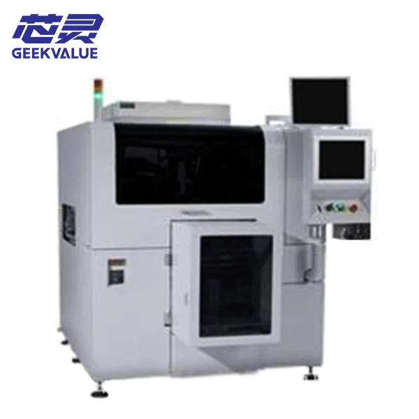
It is commonly selected by OSATs and IDMs transitioning from wire bonding and epoxy die attach processes toward flip chip architectures that enable higher I/O density and improved electrical performance.
Overview of SHIBAURA TFC-9000 Flip Chip System
The SHIBAURA TFC-9000 is used for precision flip chip die bonding in semiconductor backend manufacturing. It supports placement of silicon dies, compound semiconductors (GaAs, GaN), and optoelectronic components onto substrates, ceramic carriers, or silicon interposers.
The system is designed to support multiple bonding methodologies including mass reflow and thermocompression bonding (TCB), enabling flexible adaptation to different interconnect materials and package architectures.
Industry Applications
The TFC-9000 is applied across multiple advanced semiconductor packaging domains:
Optoelectronics & Imaging Systems
CMOS image sensors requiring high-precision optical axis alignment
VCSEL arrays for 3D sensing and optical communication modules
Micro-optical assemblies and photonic integration devices
RF & High-Frequency Devices
MMIC (Monolithic Microwave Integrated Circuits) using eutectic or flip chip interconnects
5G millimeter-wave RF front-end modules
High-frequency mixed-signal ICs requiring low parasitic interconnects
Consumer & Industrial Electronics
Application processors (AP) for mobile and computing platforms
Heterogeneous integration modules
Industrial control ICs requiring high reliability packaging
Competitive Positioning in Flip Chip Equipment
The SHIBAURA TFC-9000 is positioned as a stable mid-to-high-end flip chip bonding platform balancing precision, throughput, and process flexibility. It is commonly used in production environments scaling from mature packaging to advanced flip chip integration.
Compared to epoxy die bonders: Enables flip chip interconnects with significantly improved alignment accuracy and electrical performance.
Compared to advanced TCB platforms: Offers a more balanced solution between capital cost, throughput, and process flexibility.
Compared to legacy flip chip systems: Improves vision alignment stability, thermal control, and process repeatability for modern fine-pitch applications.
Technical Capability Overview
Precision Vision Alignment: High-resolution optical systems ensure repeatable placement accuracy for fine-pitch micro-bump structures and optical alignment requirements.
Thermal Process Control: Stable heating and cooling profiles support both mass reflow and thermocompression bonding processes.
Force Control System: Closed-loop bond head force regulation ensures consistent interconnect formation and reduces mechanical stress on delicate dies.
Flexible Substrate Handling: Compatible with laminated substrates, ceramic carriers, silicon interposers, and strip-based packaging formats.
Technical Specifications (Typical Configuration)
Performance values vary depending on process recipe, tooling setup, and device characteristics.
| Parameter | Typical Description |
|---|---|
| System Type | Fully automatic flip chip bonding platform |
| Placement Accuracy | ±2 μm to ±5 μm @ 3σ (process dependent) |
| Supported Processes | Flip chip mass reflow / Thermocompression bonding (TCB) |
| Wafer Size Support | Up to 8-inch or 12-inch (configuration dependent) |
| Substrate Compatibility | Laminated substrates, ceramic carriers, silicon interposers |
| Throughput | Varies depending on alignment complexity and bonding mode |
Why Manufacturers Choose SHIBAURA TFC-9000
Supports reliable flip chip interconnect formation for RF and optoelectronic applications
Maintains consistent alignment accuracy for fine-pitch micro-bump structures
Improves yield through controlled thermal and mechanical process stability
Enables scalable adoption of advanced packaging technologies
Advanced Semiconductor Packaging Flow
The SHIBAURA TFC-9000 is typically integrated into advanced backend packaging flows such as:
Wafer bumping/dicing → Flux application → Flip chip placement (TFC-9000) → Mass reflow / TCB → Underfill dispensing → Curing → Final electrical testing
Frequently Asked Questions
What is SHIBAURA TFC-9000 used for?
It is used for precision flip chip bonding in advanced semiconductor packaging, particularly for RF, optoelectronic, and high-density integrated circuits requiring fine-pitch interconnects.
Why choose TFC-9000 instead of standard die bonders?
It is selected when flip chip capability, higher alignment precision, and improved interconnect performance are required beyond traditional epoxy die attach processes.
Does it support thermocompression bonding (TCB)?
Yes. Depending on configuration, it supports TCB processes using dedicated bond heads, thermal modules, and precision tooling systems.
Summary
The SHIBAURA TFC-9000 flip chip bonding platform provides a balanced solution between precision, throughput, and process flexibility. It enables stable fine-pitch interconnect formation for advanced semiconductor devices used in RF, optoelectronics, and heterogeneous integration applications.
Request Technical Specification or Quotation
For manufacturers evaluating flip chip bonding equipment, detailed system configuration, process integration support, and commercial specifications are available upon request.
Equipment specification sheet
Process optimization consultation
Refurbished system availability
Production line integration support
Email / Inquiry Form Section