
Application 01
Flip Chip & Bumped Die Placement
For package structures requiring controlled die orientation, bumped interconnect and accuracy-sensitive placement.
Explore equipment directions for fine-pitch alignment, bumped-die placement, multi-die integration and high-precision semiconductor package assembly. This page focuses on the process conditions that make advanced packaging projects different from standard equipment sourcing.
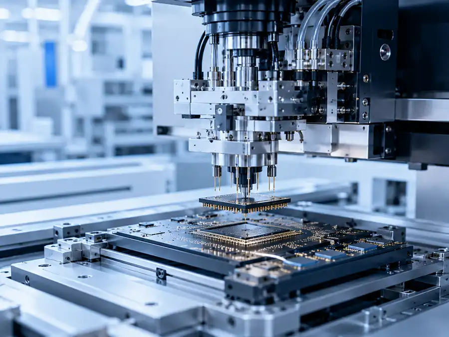
Advanced packaging projects are defined by the interconnect structure, die relationship, placement tolerance and process integration requirement—not by a single machine name alone.
For package structures requiring controlled die orientation, bumped interconnect and accuracy-sensitive placement.

For packages that integrate multiple dies, substrates or functional elements within a tightly controlled assembly route.

For alignment-sensitive interconnect layouts where placement control and repeatability become central selection factors.

For advanced structures that bring different die functions or technologies together within one package-level architecture.

This page guides the technical context. The actual equipment categories remain in their own product areas, where models, configurations and available systems can be reviewed in detail.
A high-precision packaging project should start with the package and process conditions that control placement, bonding, alignment and production stability.
Clarify die size, substrate or carrier format, package stack-up, number of dies and the physical relationship between components before selecting equipment.
Identify whether the project uses bumped die, adhesive attach, thermal process steps, wire interconnect or another defined assembly approach.
Determine the required placement tolerance, alignment strategy, vision requirement and repeatability target across the intended package structure.
Review target throughput, production flexibility, package changeover frequency and how the equipment must connect with upstream and downstream processes.
Before selecting a machine, establish the package architecture, die relationship, placement requirement, interconnect method and production objective. This creates a more focused route into the appropriate equipment category and configuration discussion.
Advanced packaging equipment supports high-precision semiconductor assembly requirements such as fine-pitch die placement, flip chip assembly, multi-die integration and complex package structures.
This Solution page explains the process requirements and technical conditions behind advanced packaging projects. The Flip Chip Bonder page focuses on the specific equipment category, available platforms and model-level sourcing direction.
Useful details include die size, substrate or carrier type, bump or interconnect requirement, placement tolerance, package construction, output target, material stack and current equipment situation.
Yes. Depending on the package architecture, a project may involve precision die placement, flip chip bonding, wire interconnect, wafer preparation and downstream package finalization equipment.
Potentially, depending on the required configuration, precision condition, process compatibility, available platform and support scope. Equipment suitability should be assessed against the actual package and production requirement.