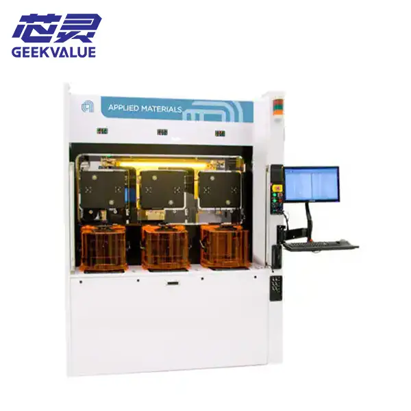
Applied Materials Raider® Edge ECD Single-Wafer Electroplating Platform
Explore the Applied Materials Raider® Edge ECD single-wafer electroplating platform for 150 mm, 200
Semiconductor electroplating systems deposit controlled metal layers for copper pillars, solder bumps, redistribution layers, TSVs, contact pads and related wafer-level structures. Browse available ECD platforms and compare the target metal, feature geometry, wafer size, chamber layout and chemistry configuration before selecting a system.
Review the electrochemical deposition platforms currently published in this category. The product page describes the model family; the actual quotation should identify the installed wafer-size hardware, chambers, chemical delivery, software and included support equipment.
Explore the Applied Materials Raider® Edge ECD single-wafer electroplating platform for 150 mm, 200
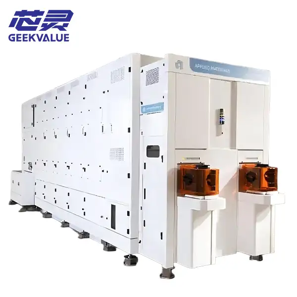
Source the Applied Materials Nokota™ ECD electrochemical deposition system for wafer-level and advan
A wafer electroplating machine is not selected by metal name alone. Copper pillars, microbumps, RDL traces, TSVs and MEMS structures impose different demands on current distribution, mass transfer, feature filling, plating thickness and post-process cleaning.
Tell us the target structure, metal stack, wafer size and production stage. We can then narrow the required chamber type, pre-wet route, wafer protection, chemistry delivery and automation level.
Controlled height, coplanarity and metal-stack requirements for flip-chip and high-density packaging.
Pattern-density and within-wafer uniformity become central when plating redistribution features.
High-aspect-ratio structures require controlled wetting, additive management and void-free fill strategy.
Gold, nickel, copper and alloy processes may support device-specific electrical or mechanical structures.
Multi-metal sequences depend on chamber separation, chemistry compatibility and wafer protection.
Search results and manufacturer product lines commonly separate manual or compact R&D tools from automated single-wafer and multi-chamber production platforms. The correct level depends on recipe maturity, wafer volume, metal separation, process sequencing and factory integration.
Higher automation does not replace process qualification, but it improves controlled handling, recipe execution, traceability and repeatability when production volume increases.
Anode zoning, current density and wafer electrical resistance influence center-to-edge deposition.
Cell geometry and flow conditions affect ion transport, feature filling and thickness consistency.
Metal concentration, additives, temperature, filtration and contamination control shape repeatability.
Continuity, resistance and surface condition can change nucleation and current distribution.
Edge exclusion, sealing and backside protection must match the wafer and process sequence.
Integrated cleaning controls chemical carryover, residue and wafer handling after deposition.
Plating quality depends on more than the machine name. The process chamber, anode design, wafer holder, electrolyte delivery, chemical management and recipe software work as one system.
For a used semiconductor electroplating system, request configuration evidence before assuming the platform can run copper pillars, TSV fill, RDL or a multi-metal stack.
Applied Materials Raider Edge and Nokota are configurable ECD platforms. A model name alone does not reveal the exact plating capability of the machine being offered.
Send your target process first. We can then compare the available system against the required wafer size, metal, chamber architecture, facilities and condition.
Check an Available ConfigurationThese answers cover the questions that usually affect equipment direction. The final recommendation still depends on the target structure and actual available system configuration.
It deposits controlled metal layers on wafers or related substrates. Common applications include copper pillars, solder bumps, redistribution layers, contact pads, TSV or TGV filling, MEMS structures and specialty metal stacks.
Manual or compact tools are commonly used for R&D, chemistry development and low-volume work. Automated systems add controlled wafer handling, recipes, pre-wet, plating, rinse, dry, traceability and multi-chamber production capability.
Potentially, but not by model name alone. Different metals may require dedicated chambers, tanks, filters, plumbing, compatible materials and contamination-control strategies. The installed configuration must be checked.
Start with feature geometry, target thickness, wafer size, seed-layer condition, metal, chemistry, uniformity target and production volume. These inputs determine the suitable cell design, flow, current control and automation route.
Inspect the chambers, anodes, wafer holders, seal components, robots, chemical tanks, pumps, filtration, plumbing, software, recipes, utilities, corrosion condition, maintenance history and decontamination status.
Send the target plated structure, metal or metal stack, wafer size, target thickness, process stage, desired automation, preferred model or manufacturer, required condition, quantity and destination country.
Share the wafer size, copper pillar, RDL, TSV, bump or specialty plating requirement, target metal, equipment condition and destination. We will review the available electroplating system configuration and the most practical supply route.