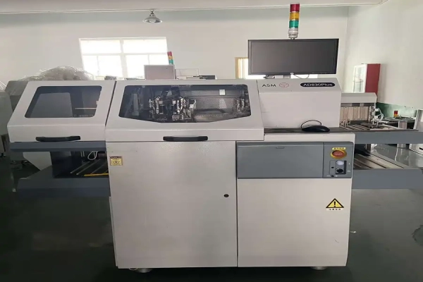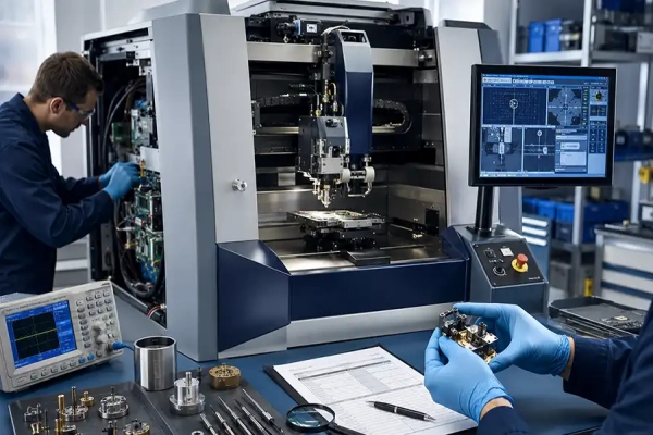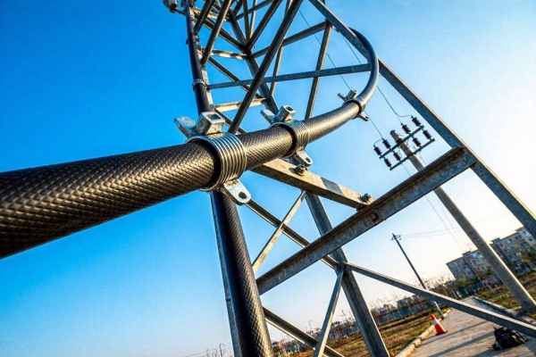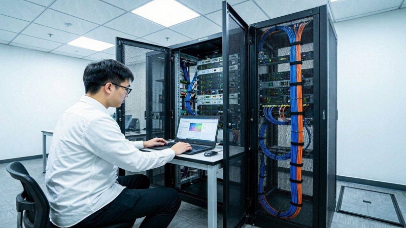
Explore how GeekValue's die bonders and flip chip bonders achieve sub-micron accuracy, high UPH, and void-free bonding for 2.5D/3D IC, automotive...
Read ArticleGeekValue Blog
Stay updated on the latest semiconductor backend equipment technologies, consumable innovations, and global support strategies.
Featured Article
High-Precision Die Bonding & Flip Chip Solutions for Advanced Semiconductor Packaging
Semiconductor Guide
ASM AD830 Plus Troubleshooting & Maintenance Guide
Diagnose ASM AD830 Plus missing-die alarms, PR failures, unstable pickup, epoxy ...
Semiconductor Guide
ASM AD830 Plus vs AD838L Plus: Die Bonder Comparison
Compare ASM AD830 Plus and AD838L Plus die bonders by material handling, substra...
Semiconductor Guide
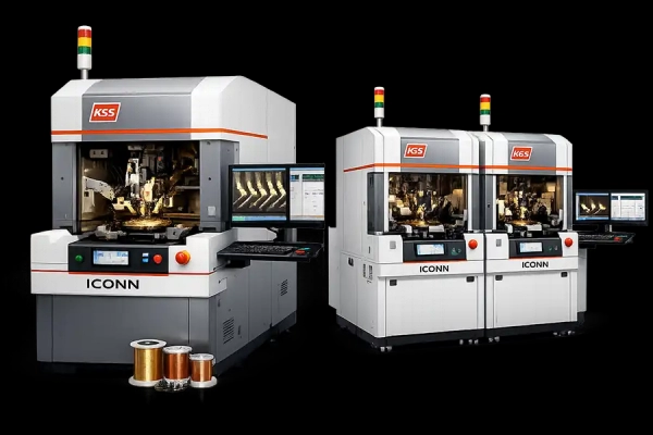
Used K&S ICONN Wire Bonder Inspection Checklist
Use this inspection checklist before buying a used K&S ICONN wire bonder. Re...
Semiconductor Guide
K&S ICONN Models Compared: ICONN, ProCu and ProCu PLUS
Compare K&S ICONN, ICONN PLUS, ICONN ProCu and ProCu PLUS wire bonders. Lear...
Semiconductor Guide
Wafer Thinning, Dicing & Cleaning for Ultra-Thin Chips: A Complete Process Guide
In-depth look at wafer backside grinding, dicing saw technology for SiC and GaN,...
Semiconductor Guide
Achieve Zero-Defect IC Testing & Final Packaging: Probe Stations, Handlers, ATE & More
How GeekValue’s automatic probe stations, test handlers, ATE systems, and final ...