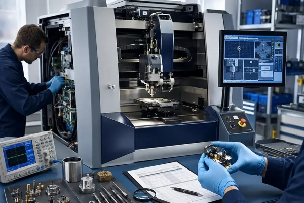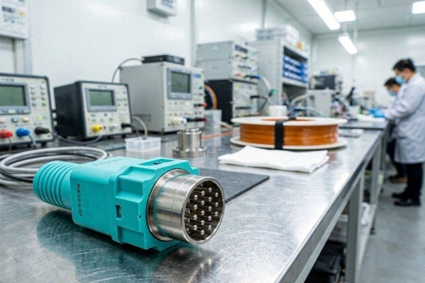
Explore how GeekValue's die bonders and flip chip bonders achieve sub-micron accuracy, high UPH, and void-free bonding for 2.5D/3D IC, automotive...
Read ArticleThe GeekValue Knowledge Base
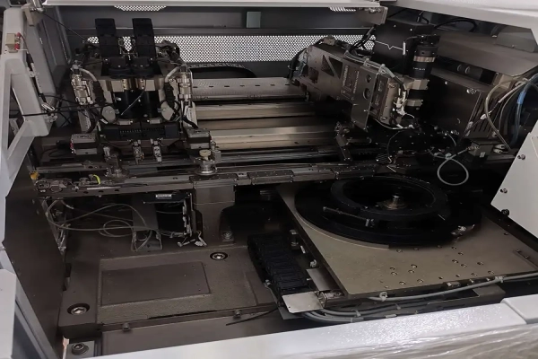
From wafer grinding and bonding to final ATE testing, explore our comprehensive collection of technical guides, best practices, and troubleshooting tutorials designed to optimize your global production lines.
Featured Article
High-Precision Die Bonding & Flip Chip Solutions for Advanced Semiconductor Packaging
Semiconductor Guide
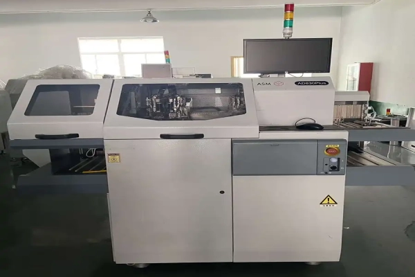
ASM AD830 Plus Troubleshooting & Maintenance Guide
Diagnose ASM AD830 Plus missing-die alarms, PR failures, unstable pickup, epoxy ...
Semiconductor Guide
ASM AD830 Plus vs AD838L Plus: Die Bonder Comparison
Compare ASM AD830 Plus and AD838L Plus die bonders by material handling, substra...
Semiconductor Guide
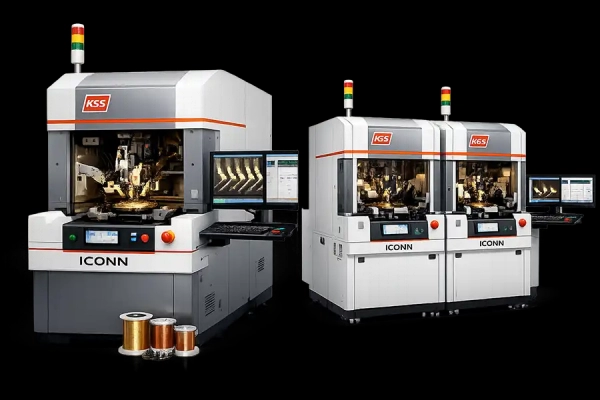
Used K&S ICONN Wire Bonder Inspection Checklist
Use this inspection checklist before buying a used K&S ICONN wire bonder. Re...
Semiconductor Guide
K&S ICONN Models Compared: ICONN, ProCu and ProCu PLUS
Compare K&S ICONN, ICONN PLUS, ICONN ProCu and ProCu PLUS wire bonders. Lear...
Semiconductor Guide
Wafer Thinning, Dicing & Cleaning for Ultra-Thin Chips: A Complete Process Guide
In-depth look at wafer backside grinding, dicing saw technology for SiC and GaN,...
Semiconductor Guide
Achieve Zero-Defect IC Testing & Final Packaging: Probe Stations, Handlers, ATE & More
How GeekValue’s automatic probe stations, test handlers, ATE systems, and final ...