Wafer-Level Identification
Mark wafer IDs, reference locations, backside codes or wafer-level traceability before dicing or downstream processing.
Typical formatWafer / Cassette
A semiconductor laser marking machine creates permanent, readable identification on wafers, molded IC packages, leadframe strips, substrates and tray-loaded devices. Use this page to compare current equipment, marking positions, code requirements, laser sources, handling formats and verification functions.
The correct laser marker depends first on what is being marked and how it reaches the marking station. Wafer ID, strip-level package marking and tray-loaded device marking require different handling, alignment and inspection architectures.
Start with the product format, mark location and code content. Laser wavelength, power, optics and automation can then be narrowed without comparing unrelated machines.
Mark wafer IDs, reference locations, backside codes or wafer-level traceability before dicing or downstream processing.
Process molded strips or substrates with rail, shuttle, magazine or strip-handling systems before singulation and final package finishing.
Mark individual ICs, MEMS or packaged devices in JEDEC trays with vision alignment, recipe control and optional code verification.
Browse the current machine collection. Product pages describe the model platform; the actual marking source, handling format, software, inspection functions and included tooling should be confirmed for the machine being supplied.
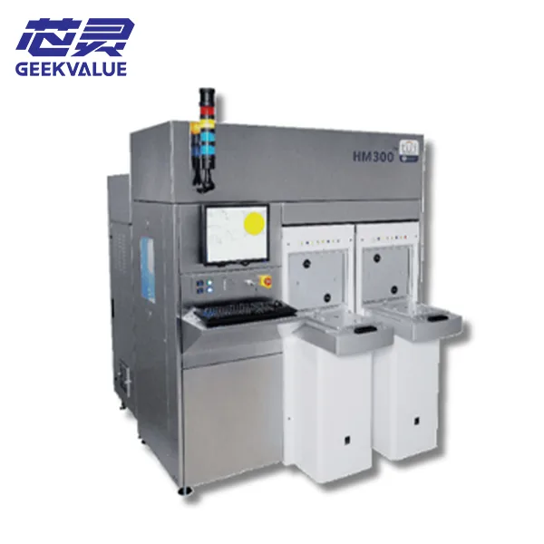
ThinkLaser HM300 automated 300 mm wafer laser marking machine for permanent hard marking, semiconduc
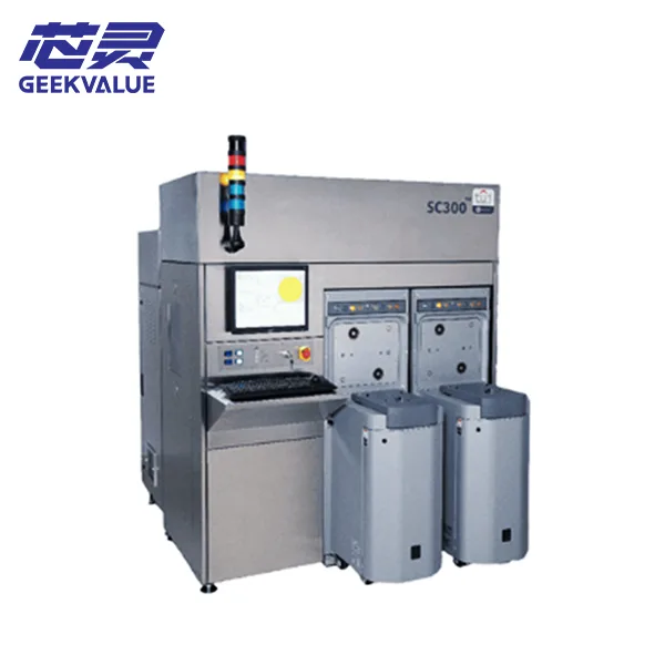
ThinkLaser SC300 automated 300 mm wafer laser marking system for debris-free soft marking, permanent
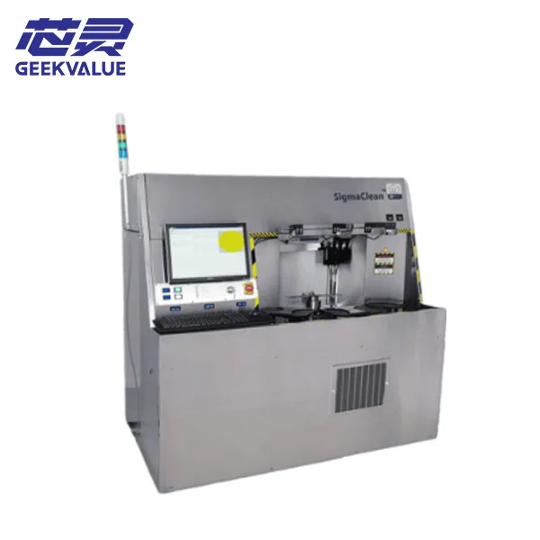
ThinkLaser SigmaClean debris-free wafer laser marking system for permanent soft marking, semiconduct
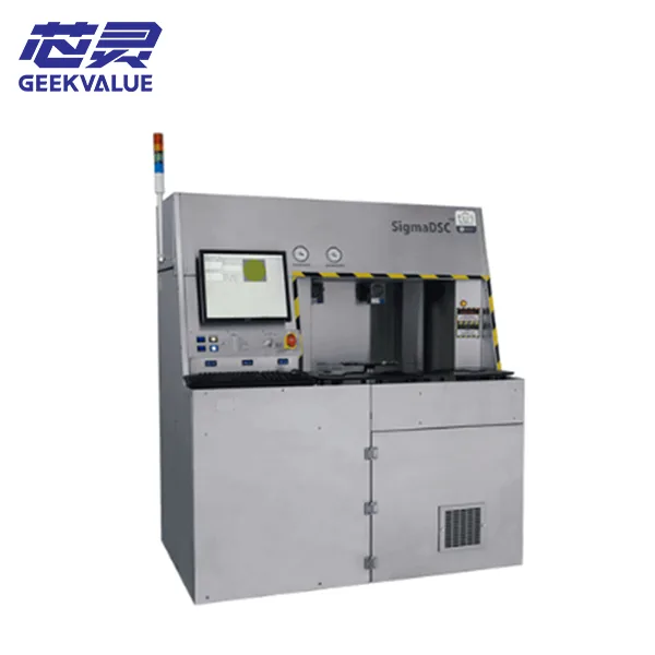
Explore the ThinkLaser SigmaDSC automated wafer laser marking system for permanent semiconductor waf
A useful comparison starts with the mark itself: human-readable text, serial numbers, logos, 1D barcodes, 2D data matrix codes or wafer IDs. The required contrast, cell size, depth and verification standard influence the laser source and optics.
The package material matters just as much. Mold compound, ceramic, silicon, metal, solder mask and coated surfaces respond differently to UV, green, infrared or fiber-based laser processing.
For semiconductor production, marking quality is only one part of the result. A complete system may also need fiducial recognition, orientation checks, OCR or data-matrix verification, duplicate-code prevention, recipe control and production-data exchange.
This is especially important for an automatic semiconductor laser marking machine connected to strip, tray or wafer handling. The installed vision hardware and software licenses must be confirmed on the actual machine.
Find fiducials, package edges or wafer reference positions before marking.
Apply the selected wavelength, pulse settings, scan path and character layout.
Check readability, content, orientation and required data-matrix quality.
Store result, lot, recipe, timestamp and equipment status when supported.
Search results cover everything from manually loaded marking workstations to high-volume semiconductor systems. The correct architecture depends on product format, takt time, lot control, inspection and connection to the surrounding line.
More automation adds controlled loading, alignment, traceability and repeatability, but it must match the package and factory interface.
Engineering, sampling, repair, small batches and flexible product changeover.
Fixture, enclosure, focus method, vision option, extraction and operator workflow.
Repeatable batch production with programmed motion, assisted loading or tray handling.
Workholder, recipe management, alignment, tray or strip format and inspection functions.
High-volume IC, strip, tray or wafer marking connected to a production line or host system.
Loader/unloader, robot, rail or shuttle, MES interface, reject handling and factory utilities.
A laser marking machine quote is more useful when it is based on the actual package and code requirement rather than laser wattage alone.
Send the information you already have. We can help identify missing points and compare them with the available system configuration.
Discuss Your Marking RequirementWafer, molded strip, leadframe, substrate, JEDEC tray or individual component determines handling architecture.
Mold compound, ceramic, silicon, metal or coated surfaces require different wavelength and process windows.
Text, logo, serial number, barcode or data matrix determines resolution, field size and verification needs.
Manual, tray, strip, magazine, wafer cassette or inline loading changes the machine architecture and quotation scope.
OCR, code grading, duplicate prevention, host communication and traceability storage may require specific cameras or licenses.
Brand, model, new/used condition, quantity, destination, voltage and project schedule help narrow current supply.
These answers cover the practical differences buyers usually need to confirm before comparing semiconductor marking systems.
Depending on the model and laser source, systems may mark molded IC packages, wafers, leadframe strips, substrates, ceramics, metals and tray-loaded components. The actual material, mark quality and handling range must be confirmed for each machine.
There is no universal source. UV, green, infrared, fiber or other solid-state laser options may be selected according to the mold compound, ceramic, silicon or metal surface, required contrast, heat sensitivity and marking speed.
Some configurable platforms support more than one format, but wafer, strip and tray handling normally require different loaders, fixtures, robots, vision routines and recipes. Confirm the installed handling modules rather than assuming multi-format capability from the laser alone.
In semiconductor packaging, the goal is usually controlled identification with readable contrast and minimal product damage. Deep engraving is not always desirable. The process depth and material interaction should match the package and traceability requirement.
Verification is valuable when the production system must confirm content, readability, orientation or duplicate-code prevention. Check whether the machine includes the required camera, illumination, software license and code-quality function.
Verify the laser source and operating hours, optics, scanner, vision system, handling modules, extraction, software version, licenses, fixtures, safety enclosure, sample-mark quality, utilities and the exact delivery scope.
Send the package or wafer format, surface material, code content, automation level and preferred machine condition. We will review the available laser marking equipment and quotation scope.