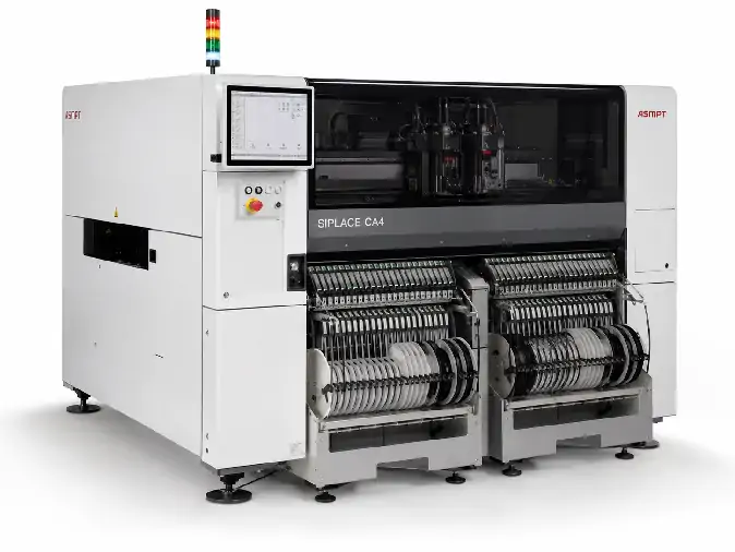
Machine de prélèvement et de placement ASMPT SIPLACE CA2
The ASMPT SIPLACE CA2 is a hybrid high-speed placement platform developed for advanced packaging production that combines conventional SMT placement with direct die placement from sawn wafers. It can process feeder-supplied SMDs and wafer-supplied dies within one connected production flow, subject to the placement heads, wafer systems, transport modules, software and process options installed on the specific machine.
For an initial inquiry, send the product or substrate dimensions, die and SMD information, wafer format, planned placement process and target production requirement. If a specific used CA2 is already under consideration, include its nameplate, configuration list, machine photos and any available operating records. Detailed tooling, software, interface and acceptance requirements can be reviewed after the candidate machine appears relevant.
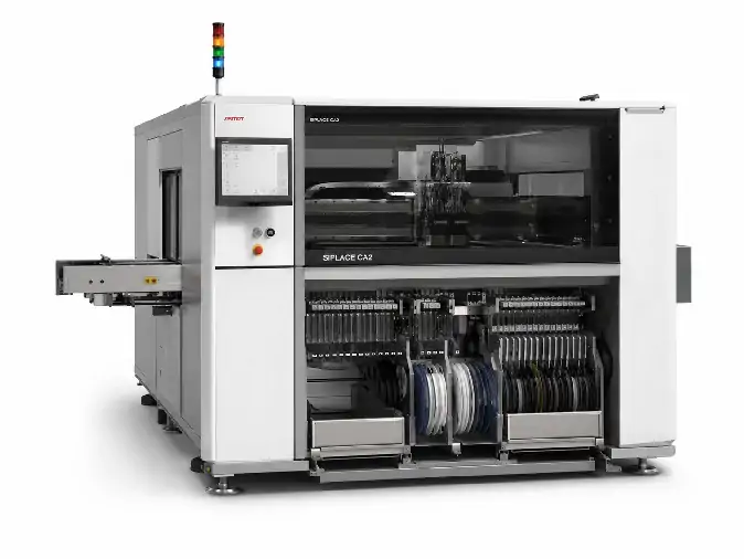
ASMPT SIPLACE CA2 Machine Information
| Fabricant | ASMPT |
|---|---|
| Modèle | SIPLACE CA2 |
| Type d'équipement | Hybrid SMT placement and direct-wafer die placement platform |
| Applications principales | System in Package, wafer-level packaging, panel-level packaging, embedded PCB assembly and compatible power semiconductor applications |
| Supported Material Streams | Feeder-supplied SMDs and dies taken directly from sawn wafers |
| Placement Processes | SMT placement, direct-wafer die attach, flip-chip placement or mixed placement, depending on configuration |
| Published SMT Placement Speed | Up to 76,000 components per hour |
| Published Die Placement from Wafer | Up to 54,000 components per hour |
| Published Flip-Chip Placement from Wafer | Up to 51,000 components per hour |
| Published Accuracy Classes | 20 µm, 15 µm and up to ±10 µm at 3 sigma, with working-area and transport limits depending on the selected class |
| Placement Head | SIPLACE CP20 reference; the installed head configuration must be confirmed on the actual machine |
| Feeder Component Range | Published CP20 range from 0201 metric to 8.2 mm × 8.2 mm × 4 mm |
| Wafer Die Range | Approximately 0.3 mm × 0.3 mm to 8.2 mm × 8.2 mm |
| Multi-Wafer Capacity | Published support for handling up to 50 different wafer types |
| Single-Track Substrate Range | Up to 620 mm × 700 mm for published 20 µm and 15 µm classes; up to 300 mm × 300 mm for the published 10 µm class |
| Dual-Track Substrate Range | Published ranges vary by accuracy class, including up to 375 mm × 260 mm at 20 µm and up to 250 mm × 100 mm at 15 µm or 10 µm |
| Factory Communication | Published support includes IPC-HERMES-9852, IPC-2591 CFX, IPC-SMEMA-9851 and SECS/GEM |
| Dimensions de la machine | Approximately 2.56 m × 2.50 m × 1.85 m |
| Condition | Pre-owned hybrid placement equipment |
| Configuration réelle | Confirmé selon la machine spécifique disponible |
| Étendue de la livraison | Sur la base du devis et de la liste des équipements confirmée |
| Soutien | Examen initial de la configuration, analyse des pannes, appariement des composants et discussion sur la réparation |
| Expédition | Emballage pour l'exportation et livraison dans le monde entier |
Hybrid SMT and Direct-Wafer Placement
The defining role of the SIPLACE CA2 is its ability to combine two material streams within one placement platform. Conventional SMDs can be supplied from compatible changeover tables and feeders, while bare dies can be picked directly from sawn wafers. This arrangement is particularly relevant when a System in Package or other advanced assembly combines IC dies with standard SMT components.
Direct placement from the wafer can remove the separate die-taping step and reduce the material handling associated with converting bare dies into tape-and-reel format. The production benefit still depends on the real component mix, the number of wafer-supplied die types, feeder demand, substrate format and downstream joining process.
Compatibilité des produits et des procédés
A SIPLACE CA2 must be matched to the full product flow rather than selected from placement speed alone. Compatibility can depend on die dimensions and thickness, wafer and frame format, feeder component range, substrate size, warpage, lane arrangement, required placement accuracy, traceability and the joining process that follows placement.
Seules des informations de base sont nécessaires pour la première discussion :
Dimensions de la puce, épaisseur, état de surface et diamètre de la plaquette
The number of wafer-supplied die types used in each product
Dimensions, quantités et exigences en matière d'alimentation des boîtiers CMS
Substrate, PCB, panel or carrier dimensions and expected warpage
The planned die-attach, flip-chip, dipping or downstream joining route
Target placement accuracy, production takt time and traceability requirement
Detailed wafer mapping, tooling, vision, software, interface and acceptance requirements can be reviewed after a specific machine configuration has been identified.
CP20 Placement Head and Component Range
ASMPT publishes the SIPLACE CP20 as the primary placement-head reference for the CA2 platform. The published range covers feeder-supplied components from 0201 metric to 8.2 mm × 8.2 mm × 4 mm and wafer-supplied dies from approximately 0.3 mm × 0.3 mm to 8.2 mm × 8.2 mm.
The published maximum performance figures describe the platform rather than every used machine. The applicable placement rate and accuracy depend on the installed heads, camera package, process mode, component geometry, substrate area, conveyor configuration, machine condition and the acceptance method used during testing.
Multi-Wafer Handling and Die Traceability
The CA2 platform supports multi-wafer production for assemblies that use several wafer-supplied die types. ASMPT publishes a wafer-handling concept for up to 50 different wafers, allowing the platform to support multi-die products without treating every die as a tape-fed component.
Available functions may include wafer exchange hardware, wafer tables or chucks, ejector systems, die buffers, wafer-map processing and individual die traceability from the original wafer position to the placement position on the substrate. These functions must be confirmed on the actual machine because the installed wafer systems, magazines, chucks, ejectors and software can differ.
Vision, Die Inspection and Dipping Options
Published CA2 options include die sensing, advanced vision, crack and edge-damage inspection, dipping control and in-line inspection. These functions can support small or sensitive components and help control the placement process, but their availability and usable inspection limits depend on the cameras, lighting, optics, sensors, software and process modules installed.
When a project requires dipping, flux transfer or another pre-placement material step, the installed Linear Dipping Unit, material reservoir, optical control and recipe capability should be checked. The presence of a dipping module does not by itself prove compatibility with a specific material, deposit volume or joining process.
Conveyor and Substrate Handling
SIPLACE CA2 can be configured with single- or dual-track transport. Published single-track ranges extend up to 620 mm × 700 mm for certain 20 µm and 15 µm configurations, while the highest published 10 µm class uses a smaller working area. Dual-track ranges also vary with the selected accuracy class.
Before purchase, confirm the installed conveyor, lane width, flow direction, left-in-left-out arrangement where applicable, substrate support, carriers and options for thick or warped products. A placement process may be technically suitable while the delivered transport system is not compatible with the actual panel or carrier.
Software, Factory Integration and Data
ASMPT publishes connectivity for IPC-HERMES-9852, IPC-2591 CFX, IPC-SMEMA-9851 and SECS/GEM, together with functions from the WORKS software environment. The platform can also support material automation, recipe preparation, production data and closed-loop functions when the required software, interfaces and measurement equipment are available.
A listed communication standard should not be treated as proof that a used machine is ready for a particular MES or traceability system. Confirm the software release, active licenses, computer and controller condition, recipe backups, wafer-map functions, data interfaces and any transferable documentation for the offered unit.
Available SIPLACE CA2 Configuration and Delivery Scope
Individual ASMPT SIPLACE CA2 machines may differ in CP20 head configuration, camera and sensor packages, Multi Wafer Systems, wafer exchange equipment, chucks, ejectors, die buffers, dipping units, feeder tables, JEDEC tray options, conveyor arrangement, inspection modules, software, licenses and factory interfaces. Before purchase, the available machine should be reviewed against the intended die, SMD, substrate and production flow. The final delivery scope is based only on the quotation and confirmed equipment list; wafer hardware, feeders, trays, tools, carriers, computers, software, documentation, spare parts and external utility equipment are included only when specifically stated.
Réception, mise en service et contrôle initial des échantillons
The SIPLACE CA2 should be inspected and tested in stages before valuable wafers, dies or production substrates are introduced.
Inspect the packing, machine frame, cabinets, conveyor, feeder areas, wafer modules, placement heads, cameras, guards and control equipment.
Photographiez toutes les marques d'impact, les assemblages desserrés, les câbles endommagés ou les composants de positionnement et de plaquette déplacés avant de déplacer la machine.
Compare the received machine, wafer systems, chucks, ejectors, feeder tables, dipping equipment, tools and accessories with the confirmed delivery list.
Confirm the electrical supply, grounding, compressed air, vacuum, exhaust, network and environmental requirements of the actual configuration.
Démarrez le contrôleur et enregistrez tous les messages d'alarme avant de réinitialiser le système ou de modifier les données de la machine.
Run the conveyor, placement axes, feeder interfaces and wafer-handling mechanisms without production material.
Check wafer loading, die ejection, pickup, vision recognition, optional dipping and placement with non-production or representative samples.
Verify substrate transport, placement sequence, traceability and any required software or factory communication functions.
A powered-on dry cycle confirms only part of the machine condition. Representative material and an agreed acceptance method are needed when the purchase decision depends on die pickup stability, vision performance, placement accuracy or a specific mixed SMD-and-die process.
Défauts de placement, manipulation des plaquettes et assistance technique
Pickup failures, die rotation, vision rejects or unstable placement can involve wafer tension, ejector setup, pickup tooling, contamination, lighting, focus, calibration, recipe settings or die-surface conditions. Feeder or substrate faults may involve reel setup, feeder communication, conveyor alignment, board support, carriers or warped products.
Software and traceability issues may involve wafer-map orientation, coordinate conversion, licenses, recipe files, network settings or external interfaces. Record the alarm message and the exact process stage before resetting the machine. Photos of the wafer, die, substrate, tooling and alarm screen, together with a short operating video where available, can provide a practical starting point for review.
Our team can assist with initial fault analysis, component identification, replacement-part matching and repair discussion. Related cameras, sensors, motors, drivers, boards, cables, vacuum parts, feeder components, wafer-handling assemblies, ejector parts, tools and product fixtures can also be checked where available.
Foire aux questions
Is the ASMPT SIPLACE CA2 an SMT machine or a die bonder?
It is a hybrid placement platform that combines conventional SMT placement with direct pickup and placement of dies from sawn wafers. The available SMD, die-attach and flip-chip functions depend on the installed machine configuration.
Can the SIPLACE CA2 place SMDs and bare dies in the same production flow?
Yes. This mixed material flow is the defining purpose of the CA2 platform. The actual balance between wafer systems, feeder positions and transport options must still be confirmed for the offered machine.
Does every SIPLACE CA2 achieve ±10 µm placement accuracy?
No. ASMPT publishes several accuracy classes, including 20 µm, 15 µm and up to ±10 µm at 3 sigma. The applicable class and working area depend on the installed configuration, product geometry, transport arrangement and acceptance method.
How many wafer types can the CA2 handle?
ASMPT publishes a multi-wafer concept for up to 50 different wafer types. The actual capacity of a used machine depends on its installed wafer exchange equipment, magazines, chucks, ejectors and software.
Is the SIPLACE CA2 automatically suitable for thermocompression bonding?
No. The platform supports direct-wafer die attach and flip-chip placement, but thermocompression bonding requires suitable heat, force, atmosphere, tooling and process-control equipment. The intended joining process must be evaluated separately.
Can you assist with CA2 alarms, configuration questions or replacement parts?
Yes. Send the full model information, alarm message, machine and module photos and a short operating video where available. We can assist with initial configuration review, fault analysis, component matching and repair discussion.
Contact Us About the ASMPT SIPLACE CA2
Send the die and wafer information, SMD list, substrate dimensions, planned placement process, target accuracy and production requirement. If a specific machine is already available, include its nameplate, configuration list, photos and operating evidence. We will review the basic application first and continue with the required placement head, wafer system, transport, software, tooling, replacement-parts or repair details afterward.