The TEL CELLESTA™-i MD wafer cleaner is an advanced single wafer cleaning system developed for semiconductor manufacturing processes requiring high cleanliness, excellent process control, and stable wafer yield performance.
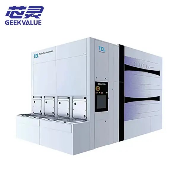
Designed for 300mm wafer production, the CELLESTA™-i MD supports advanced semiconductor manufacturing where particle removal, surface contamination control, and pattern protection are critical factors affecting device performance and reliability.
As semiconductor technology continues moving toward smaller process nodes and more complex device structures, wafer cleaning has become one of the most important processes in semiconductor fabrication. Advanced cleaning equipment must remove contamination while protecting delicate wafer patterns.
What is TEL CELLESTA™-i MD Wafer Cleaner?
The TEL CELLESTA™-i MD is a single wafer cleaning system used in front-end semiconductor manufacturing. Unlike batch cleaning equipment that processes multiple wafers simultaneously, single wafer cleaning provides individual wafer process control with improved cleaning uniformity and repeatability.
The system is designed for advanced semiconductor processes where even microscopic particles or surface residues can negatively impact device performance and production yield.
Typical applications include logic semiconductor manufacturing, memory production, and advanced wafer processes requiring precise contamination control.
Why Semiconductor Wafer Cleaning is Critical
During semiconductor fabrication, wafers experience hundreds of process steps including lithography, etching, deposition, and implantation. These processes can introduce different types of contamination.
Particle contamination
Organic residues
Metal contamination
Chemical residues
Etching by-products
Without effective cleaning, contamination may cause electrical defects, reduced yield, device reliability problems, and shortened product lifetime.
TEL CELLESTA™-i MD Key Technologies
300mm Single Wafer Processing
The CELLESTA™-i MD is designed for 300mm wafer manufacturing environments. Single wafer processing allows precise control of chemical exposure, cleaning conditions, and drying performance.
Advanced Particle Removal
The system provides high-performance particle removal while minimizing damage to sensitive semiconductor structures. This capability is important for advanced devices with smaller geometries and complex patterns.
Pattern Collapse Prevention Technology
As semiconductor patterns become smaller, wafer drying becomes increasingly challenging. Excessive surface tension during drying can damage fine structures.
The CELLESTA™-i MD incorporates advanced drying technology to reduce pattern collapse risks and support next-generation semiconductor manufacturing.
High Process Stability
Advanced semiconductor production requires stable cleaning performance across thousands of wafers. The CELLESTA™-i MD focuses on repeatability, process control, and manufacturing consistency.
TEL CELLESTA™-i MD Applications
Advanced Logic Semiconductor Manufacturing
Modern logic chips require extremely low contamination levels. The CELLESTA™-i MD supports cleaning processes where particle control directly impacts yield improvement.
Memory Semiconductor Production
High-density memory devices require precise wafer cleaning to maintain structure integrity and manufacturing reliability.
Post Etch Cleaning
After plasma etching processes, wafer surfaces may contain residues requiring controlled cleaning before the next fabrication step.
Metal Layer Cleaning
Advanced semiconductor devices often contain exposed metal structures that require careful cleaning without damaging sensitive materials.
TEL CELLESTA™-i MD Technical Specifications
| Parameter | Description |
|---|---|
| Equipment Type | Single wafer cleaning system |
| Manufacturer | Tokyo Electron (TEL) |
| Model | CELLESTA™-i MD |
| Wafer Size | 300mm |
| Process Type | Wet wafer cleaning |
| Main Function | Particle removal and surface cleaning |
| Application | Advanced semiconductor manufacturing |
| Target Market | Logic, memory and advanced semiconductor fabs |
TEL CELLESTA™-i MD Cleaning Process Flow
Wafer loading
Chemical cleaning process
Particle and residue removal
DI water rinse
Advanced drying process
Wafer inspection and transfer
Process Flow:
Wafer Loading → Chemical Cleaning → Rinse → Drying → Inspection → Next Semiconductor Process
TEL CELLESTA™-i MD Advantages
High cleaning accuracy for advanced semiconductor nodes
Excellent particle removal capability
Reduced wafer damage risk
Stable 300mm wafer production performance
Suitable for high-volume semiconductor manufacturing
TEL CELLESTA™-i MD vs Other Semiconductor Cleaning Equipment
| Equipment Type | Main Application |
|---|---|
| TEL CELLESTA™-i MD | Front-end 300mm wafer cleaning |
| SC810 Package Cleaner | Post-solder semiconductor package cleaning |
| Plasma Cleaner | Surface activation and contamination removal |
The CELLESTA™-i MD belongs to front-end semiconductor fabrication equipment, while package cleaning and plasma systems are mainly used in backend assembly and surface treatment processes.
Maintenance Considerations
Maintaining stable cleaning performance is essential for semiconductor manufacturing yield. Regular maintenance usually includes:
Chemical supply inspection
Cleaning chamber maintenance
Nozzle inspection
Drying system verification
Process recipe calibration
Particle performance monitoring
Summary
The TEL CELLESTA™-i MD wafer cleaner is an advanced 300mm single wafer cleaning solution designed for modern semiconductor manufacturing.
With precise cleaning control, advanced particle removal capability, and optimized wafer protection technology, the CELLESTA™-i MD helps semiconductor manufacturers improve production yield and support next-generation chip development.