The commercialization of micro LED displays and advanced RF front-end modules is driving semiconductor packaging toward a new requirement: combining sub-micron placement accuracy with mass-production throughput. The Kulicke & Soffa (K&S) Katalyst™ flip chip mounter is designed to address this manufacturing gap.
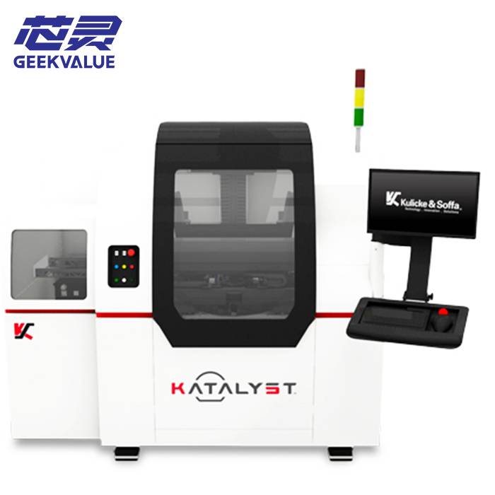
Unlike conventional die bonders optimized for large silicon dies, the Katalyst platform is engineered for ultra-small die assembly, including micro LEDs and compound semiconductor RF devices, enabling scalable production of next-generation optoelectronic systems.
Core Process Capability Overview
High-Speed Mass Transfer: Supports rapid placement of micro-scale dies with controlled motion dynamics.
Sub-Micron Vision Alignment: Optical recognition system compensates for substrate distortion and die variation.
Precision Force Control: Closed-loop bond head regulation prevents die damage and bump collapse.
Advanced Thermal Control: Supports eutectic and thermocompression bonding (TCB) profiles.
Mass Transfer & Motion Architecture
The Katalyst system is optimized for high-speed die transfer operations, reducing non-productive motion time while maintaining alignment stability. This enables efficient placement of thousands of micro components in display-scale manufacturing environments.
The motion system is designed to balance acceleration and stability, ensuring consistent die placement without inducing vibration-induced misalignment.
Application Domains
Micro LED Display Manufacturing
Mass transfer of RGB micro LED arrays
AR/VR and wearable display integration
Large-area display backplane assembly
RF & 5G Semiconductor Modules
Millimeter-wave front-end modules
RF filters and power amplifiers
Low-parasitic compound semiconductor interconnects
Optoelectronics & Sensing
VCSEL arrays for 3D sensing and LiDAR
CMOS image sensor integration
Photonic and hybrid optical modules
Technical Specification (Typical Range)
| Parameter | Specification |
|---|---|
| System Type | High-speed flip chip / mass transfer mounter |
| Placement Accuracy | Sub-micron to ±2 μm @ 3σ (process dependent) |
| Bonding Methods | TCB / Eutectic / Advanced mass transfer |
| Target Die Size | Ultra-small dies (micro LED / RF / photonics) |
| Substrate Compatibility | Display backplanes / organic laminates / ceramic carriers |
| Throughput | Optimized for high-volume display manufacturing |
Process Flow Integration
Wafer fabrication → Dicing → Mass transfer preparation → High-speed placement (Katalyst) → Eutectic / TCB bonding → Testing → Module assembly
Engineering Evaluation
What makes Katalyst different from standard flip chip bonders?
Standard flip chip systems focus on medium-to-large silicon dies. Katalyst is optimized for ultra-small die arrays, especially micro LEDs, requiring both extreme precision and high-throughput scalability.
Is it suitable for micro LED mass production?
Yes. The system is specifically designed to bridge laboratory-level micro LED assembly and industrial-scale display manufacturing.
Which bonding methods are supported?
It supports eutectic bonding and thermocompression bonding (TCB), enabling both optical and RF-grade interconnect reliability.
Summary
The Kulicke & Soffa (K&S) Katalyst flip chip mounter enables scalable manufacturing of micro LED and advanced RF devices by combining high-throughput mass transfer with sub-micron alignment and advanced thermal bonding control. It is a key platform for next-generation optoelectronic and communication packaging.
Request Technical Specification or Quotation
Equipment specification sheet
Micro LED / RF process compatibility report
System configuration options
Production integration consulting
Contact engineering team for evaluation or quotation support.