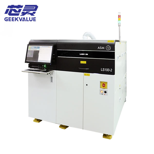
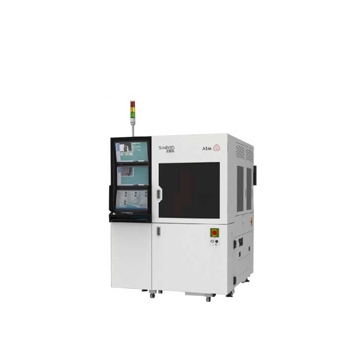
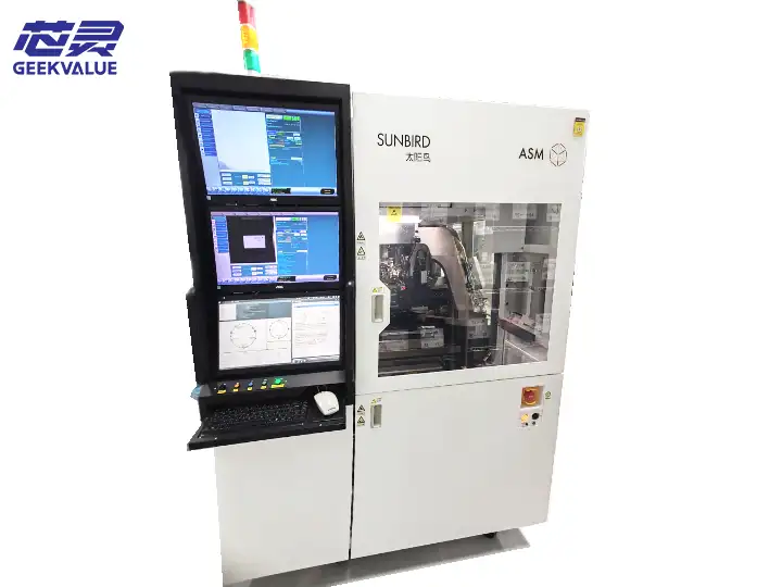
The ASM AD819 is a high-precision automatic die bonding system designed for semiconductor backend packaging processes where alignment accuracy and process control are critical. It is typically used in production environments that prioritize placement precision over high-throughput manufacturing.
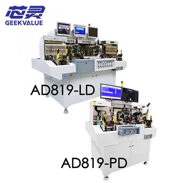
Key application areas include optoelectronic devices, CMOS image sensors, RF components, medical sensors, and precision discrete semiconductor packaging.
Overview of ASM AD819 Die Bonding System
The ASM AD819 is a fully automatic die attach platform used to place semiconductor dies onto substrates or leadframes with high positional accuracy. It is designed for applications where alignment tolerance directly impacts optical, electrical, or thermal performance.
Compared to general-purpose high-speed die bonders, the AD819 is optimized for precision control, stable repeatability, and fine alignment capability across complex device structures.
Supported Die Bonding Processes
The system supports multiple die attach processes depending on configuration and tooling setup:
-
Epoxy Die Attach: Used for precision adhesive bonding in sensor and discrete semiconductor packaging, where controlled dispensing and alignment are required.
-
Eutectic Bonding: Applied in RF and high-frequency applications using AuSn or similar alloys to improve thermal conductivity and electrical performance.
-
Flip Chip Attach (Optional Configuration): Supports face-down die placement for high-density interconnect structures depending on module setup.
Technical Characteristics (Typical Configuration)
Performance varies depending on bonding module, process setup, die size, and substrate type.
| Parameter | Typical Description |
|---|---|
| System Type | Automatic high-precision die bonder |
| Placement Accuracy | ±3 μm to ±5 μm @ 3σ (process dependent) |
| Throughput | Dependent on bonding method and alignment complexity |
| Wafer Handling | Up to 8-inch or 12-inch (configuration dependent) |
| Substrate Compatibility | Leadframes, laminated substrates, strip carriers |
| Bonding Methods | Epoxy / Eutectic / Flip Chip (module dependent) |
Applications in Semiconductor Packaging
The ASM AD819 is commonly used in semiconductor packaging processes that require high placement accuracy and stable bonding quality.
Optoelectronics and Imaging Devices
-
CMOS image sensors requiring precise optical alignment
-
VCSEL and photonic components
-
MEMS-based sensing devices
RF and Communication Devices
-
RF filters and high-frequency amplifiers
-
Mixed-signal integrated circuits
-
Devices requiring eutectic bonding for thermal stability
Medical and Precision Semiconductor Devices
-
Medical sensing chips
-
Low-power diagnostic semiconductor devices
-
High-reliability discrete components
Backend Semiconductor Process Integration
In semiconductor manufacturing flows, the AD819 is typically positioned after wafer dicing in the backend assembly process.
Following die attach, devices proceed to wire bonding, encapsulation, and final testing stages. The system is designed to integrate with standard leadframe and strip-based production lines as well as customized handling systems used in precision manufacturing environments.
Frequently Asked Questions (FAQ)
What is the ASM AD819 used for?
It is used for high-precision die attach processes in semiconductor packaging, particularly where alignment accuracy is critical for device performance.
How is it different from high-speed die bonding systems?
Unlike high-speed systems optimized for maximum throughput, the AD819 is designed for precision placement, making it suitable for optoelectronic, RF, and sensor applications.
Can it support different bonding technologies?
Yes, the platform supports multiple bonding methods, but switching between processes requires specific tooling and configuration modules.
Summary
The ASM AD819 is a precision-focused die bonding system designed for semiconductor applications where alignment accuracy and process stability are more important than maximum production speed. It is widely used in optoelectronics, RF devices, and high-reliability semiconductor packaging.