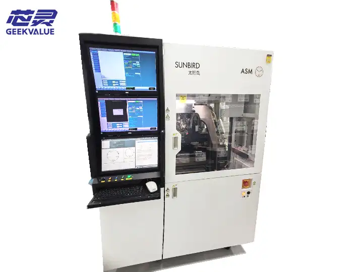
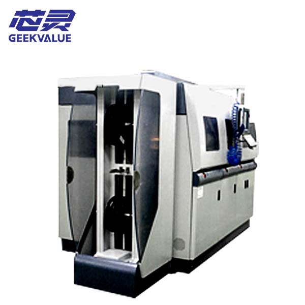
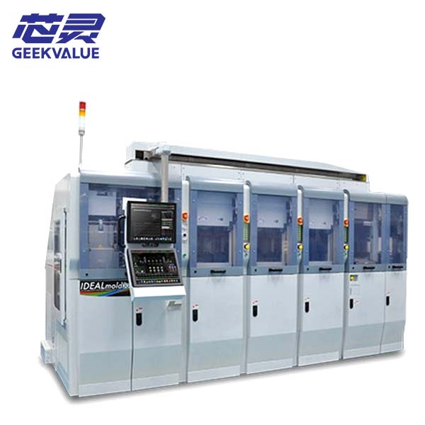
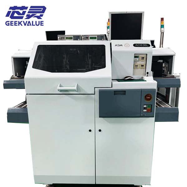
The ASMPT AD211 Plus is a fully automatic eutectic die bonding system designed for semiconductor backend manufacturing processes that require high thermal conductivity, strong electrical performance, and long-term reliability.
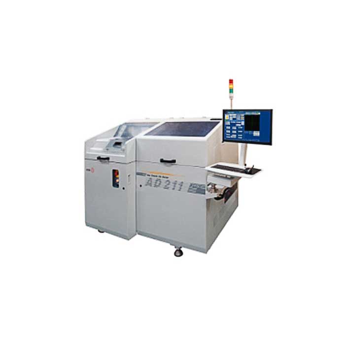
It is engineered specifically for metallurgical interconnect applications using AuSn or compatible solder alloys, enabling stable die attach for RF, optoelectronic, and power semiconductor devices operating under high thermal stress conditions.
It is widely used by OSATs and IDMs transitioning from epoxy die attach processes to advanced eutectic bonding solutions for high-power and high-frequency applications.
What is ASMPT AD211 Plus?
The ASMPT AD211 Plus is a fully automatic eutectic die attach platform used in semiconductor packaging to form metallurgical bonds between semiconductor dies and substrates.
It processes silicon or compound semiconductor dies such as GaAs and GaN, attaching them to leadframes or ceramic substrates using controlled reflow of AuSn or Sn-based solder systems.
Unlike epoxy die bonding, eutectic bonding creates a direct metal-to-metal interconnect, significantly improving thermal conductivity and electrical performance.
Manufacturing Role in Semiconductor Packaging
The AD211 Plus is positioned as a specialized eutectic die bonding solution for high-reliability semiconductor manufacturing.
It is typically used in production environments where thermal dissipation, electrical stability, and long-term device durability are more critical than cost-optimized epoxy bonding.
Industry Applications
The ASMPT AD211 Plus is widely deployed in high-reliability semiconductor packaging sectors:
RF and Microwave Devices
RF power amplifiers using AuSn eutectic die attach
MMIC (Monolithic Microwave Integrated Circuits)
5G and millimeter-wave front-end modules
Optoelectronics and Photonics
Laser diode and VCSEL assemblies
Optical transceivers and photonic modules
High-power LED components requiring thermal stability
Power Semiconductor Devices
High-power MOSFETs and IGBTs (select configurations)
Automotive-grade power discrete devices
Thermally critical power management modules
Competitive Positioning in Die Bonding Equipment
The ASMPT AD211 Plus is positioned as a high-precision eutectic bonding platform for advanced semiconductor packaging applications.
Compared to epoxy die bonders: delivers significantly improved thermal conductivity and lower junction temperature due to metallurgical interconnects
Compared to manual solder processes: provides automated control of reflow, pressure, and alignment for consistent mass production quality
Compared to advanced sintering systems: offers a mature, cost-efficient eutectic bonding solution with proven industrial adoption
Core Technical Capabilities
Eutectic Reflow Control: Precise temperature and time profiling ensures stable AuSn or Sn-based phase formation during bonding.
Atmosphere Management System: Controlled forming gas (N₂ or N₂/H₂ depending on configuration) reduces oxidation and improves wetting behavior.
Force & Scrub Control: Programmable bonding force and motion profiles minimize void formation and improve interfacial quality.
High-Resolution Vision Alignment: Ensures accurate die placement under molten or semi-molten bonding conditions.
Technical Specifications (Typical Configuration)
Actual performance depends on die type, solder material, substrate design, and process recipe configuration.
| Parameter | Description |
|---|---|
| System Type | Fully automatic eutectic die bonder |
| Bonding Process | AuSn / SnAg eutectic reflow bonding |
| Placement Accuracy | ±5 μm to ±10 μm @ 3σ (process dependent) |
| Void Level | <5% typical (depends on die size and process optimization) |
| Atmosphere Control | Programmable inert or forming gas environment |
| Throughput | Optimized for RF and power device mass production |
Why Manufacturers Use ASMPT AD211 Plus
Improves thermal management in high-power semiconductor devices
Enables reliable metallurgical interconnect formation for RF applications
Reduces process variability compared to manual soldering methods
Supports long-term reliability requirements in automotive and telecom industries
Semiconductor Backend Process Flow
Wafer dicing → Solder / flux preparation → Eutectic die attach (ASMPT AD211 Plus) → Reflow → Cleaning → Wire bonding → Final testing
Frequently Asked Questions
What is ASMPT AD211 Plus used for?
It is used for eutectic die attach in RF, optoelectronic, and power semiconductor packaging, enabling metallurgical bonding with high thermal and electrical performance.
Why use eutectic bonding instead of epoxy die attach?
Eutectic bonding provides significantly higher thermal conductivity and electrical performance compared to epoxy adhesives, making it suitable for high-power and high-frequency devices.
Is the process completely void-free?
No solder or eutectic process is completely void-free, but the system is engineered to maintain low void levels (typically below 5%) through controlled atmosphere and optimized bonding profiles.
Summary
The ASMPT AD211 Plus is a high-reliability eutectic die bonding system designed for advanced semiconductor packaging applications requiring superior thermal and electrical performance.
It is widely used in RF, optoelectronics, and power semiconductor manufacturing where metallurgical interconnect quality directly impacts device lifetime and performance stability.
Request Technical Specification or Quotation
For manufacturers evaluating eutectic die attach equipment for high-reliability semiconductor production, detailed configuration options, tooling specifications, and commercial terms are available upon request.
Equipment specification sheet
Process configuration assessment
Refurbished machine availability
Production line integration support
Email / Inquiry Form Section