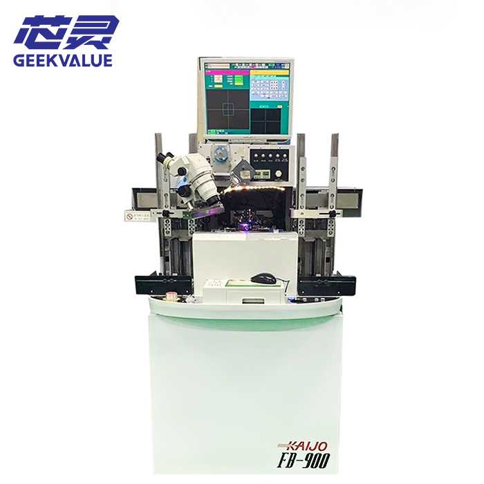
A semiconductor flip chip placement machine is a backend packaging system designed to mount bare dies face-down onto substrates, ceramic carriers, or silicon interposers using micro-bump interconnects. Compared with wire bonding or epoxy die attach, flip chip technology enables shorter signal paths, higher I/O density, and improved thermal performance.
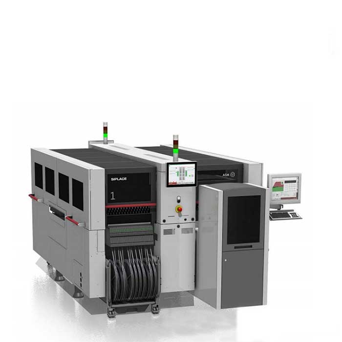
As advanced packaging evolves toward heterogeneous integration and 2.5D/3D architectures, flip chip placement equipment becomes a core decision point in both process design and production scaling.
Core System Modules
Vision & Alignment System
High-resolution optical recognition for die bumps and substrate pads
Real-time compensation for substrate warpage and die offset
Sub-micron or micron-level alignment depending on system class
Placement & Force Control
Closed-loop bond head force regulation
Prevention of bump collapse and die cracking
Uniform contact across full die surface during placement
Flux & Interconnect Management
Precision flux dipping or jet dispensing systems
Controlled volume application to reduce void formation
Stable solder joint formation during reflow
Thermal Process Control
Mass reflow stage heating for high-throughput systems
Localized heating for thermocompression bonding (TCB)
Optimized thermal profiles for solder alloys and substrates
Process Selection: Mass Reflow vs TCB
Mass Reflow Systems
Best for pitch >100 μm
High throughput (consumer and mobile IC production)
Uses flux + off-line reflow oven process
Thermocompression Bonding (TCB)
Best for sub-40 μm fine-pitch interconnects
Required for 2.5D/3D heterogeneous integration
Localized heat + force applied during bonding
Application Areas
High-Performance Computing (HPC)
AI accelerators and GPU packaging
Chiplet-based architectures
HBM integration
Mobile & Consumer Devices
Application processors (AP)
Smartphones and wearable electronics
RF & Optoelectronics
5G RF front-end modules
CMOS image sensors and VCSEL arrays
Co-packaged optics (CPO)
Technical Specifications (Industry Ranges)
| Parameter | Mass Reflow | TCB |
|---|---|---|
| Placement Accuracy | ±5 μm to ±15 μm @ 3σ | ±0.5 μm to ±2 μm @ 3σ |
| Supported Pitch | >100 μm | Sub-40 μm to 100 μm |
| Bonding Method | Flux + reflow oven | Localized heat + force |
| Throughput | High (5,000–15,000 UPH) | Medium to low (precision-driven) |
| Substrate Types | Organic laminates, leadframes | Silicon interposers, ceramics, organic substrates |
Manufacturing Flow Integration
Flip chip placement machines are positioned as the core interconnect formation step in advanced backend packaging.
Wafer bumping → Wafer dicing → Flux application → Flip chip placement → Reflow / TCB → Underfill → Curing → Final test
Engineering Notes
Key Selection Factor
The main selection driver is the trade-off between throughput (mass reflow) and precision (TCB).
Common Limitation
Mass reflow: limited by pitch scaling and warpage sensitivity
TCB: lower throughput due to thermal cycle time
Best Practice
Match equipment type directly to interconnect pitch and packaging architecture rather than production volume alone.
Summary
Semiconductor flip chip placement machines are essential for modern advanced packaging, enabling high-density interconnects required for AI, mobile, RF, and heterogeneous integration systems. Proper selection between mass reflow and TCB platforms directly determines yield, scalability, and device performance.
Request Technical Documentation
Equipment specification sheet
Process compatibility analysis
TCB vs Mass Reflow selection guide
Production line integration support
Contact engineering team for technical evaluation or quotation support.