The ASMPT SIPLACE CA2 is a hybrid high-speed placement platform that processes conventional surface-mount components and bare semiconductor dies in the same production environment. It can pick SMDs from tape-and-reel feeders while also taking dies directly from a diced wafer.
This combination makes the CA2 relevant to System-in-Package production, multi-die modules, wafer- and panel-level packaging, embedded components and selected power-semiconductor applications. Its strongest value appears when direct-wafer placement is a meaningful part of the product rather than an occasional specialist operation.
The machine should not be selected from one speed or accuracy figure alone. The real decision depends on the balance between wafer-supplied dies and feeder-supplied components, the number of die types, the substrate format, the required joining route and the installed CA2 configuration.
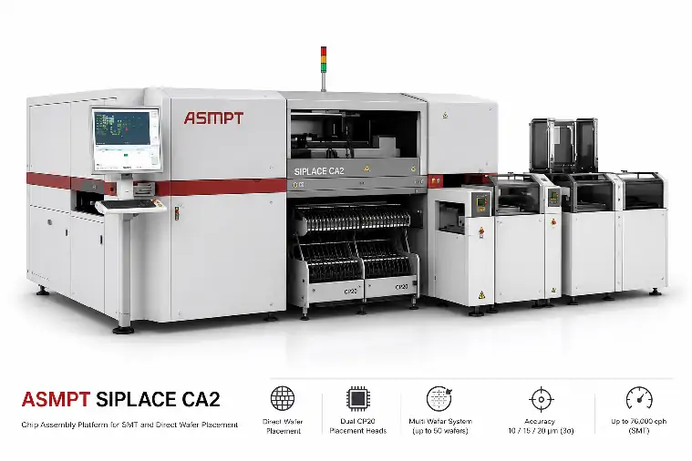
What the SIPLACE CA2 Is Designed to Do
A conventional SMT placement machine normally receives packaged components from tape, trays or other feeders. A die-placement system must instead identify and retrieve singulated dies from a wafer, maintain their source information and transfer them to a substrate or package.
The SIPLACE CA2 brings these two material flows into one platform. Depending on configuration, it can support:
SMD placement from tape-and-reel feeders
Direct pickup of bare dies from diced wafers
Die-attach placement before the qualified joining process
Face-down flip-chip placement
Mixed products containing several dies and selected SMT components
Direct wafer feeding can remove the intermediate die-taping step. This can reduce the material preparation, replenishment and handling associated with transferring sensitive dies into tape before placement. The production benefit is greatest when a product family uses several wafer-supplied components or requires frequent switching between die types.
The CA2 is therefore not simply an SMT machine with an additional wafer input. Its placement heads, wafer exchange, die buffering, vision, material handling and traceability functions are arranged around mixed semiconductor and SMT assembly.
Published SIPLACE CA2 Specifications
The following values describe ASMPT's published platform capability. Maximum speed and accuracy depend on the operating mode, placement position, component geometry, conveyor arrangement and selected options. The specification table defines a possible process window rather than predicting the cycle time or condition of an individual machine.
| Specification Area | Published CA2 Capability | Practical Meaning |
|---|---|---|
| Placement architecture | Two SIPLACE CP20 placement heads | The two-head platform supports high-speed SMT and direct-wafer placement. |
| SMT placement benchmark | Up to 76,000 cph | The value represents platform direction rather than guaranteed product output. |
| Flip-chip placement from wafer | Up to 51,000 cph | The real rate also depends on wafer pickup, vision, dipping and substrate indexing. |
| Die attach from wafer | Up to 54,000 cph | This reflects the platform's emphasis on high-volume direct-wafer processing. |
| Placement accuracy classes | 20 µm, 15 µm or 10 µm at 3 sigma | The class can be assigned according to placement position and component shape. |
| Tape-fed component range | 0201 metric to 8.2 mm × 8.2 mm | Components outside this range require another placement solution or a divided line process. |
| Wafer-supplied die range | 0.3 mm × 0.3 mm to 8.2 mm × 8.2 mm | Die thickness, pickup surface, bump structure and handling stability still need evaluation. |
| Wafer handling | Up to 50 different wafers; swap time approximately 13 seconds | The architecture supports products that require frequent changes among several die sources. |
| Material configurations | Up to 80 × 8 mm feeder positions, or up to two Multi Wafer Systems with 10 × 8 mm feeder tracks | The required balance between wafer capacity and conventional feeder positions must be defined first. |
| Single-lane substrate range | Up to 700 mm × 620 mm at selected accuracy classes; up to 300 mm × 300 mm at 10 µm | Large-panel handling and highest-accuracy placement do not use the same full working area. |
| Machine dimensions | 2.56 m × 2.50 m × 1.85 m | Line planning must also include loading, service and material-access space. |
| Factory interfaces | IPC-HERMES-9852, IPC-CFX, IPC-SMEMA-9851 and SECS/GEM | The delivered software version and licensed functions determine actual implementation. |
| Compliance information | CE and SEMI S2/S8 listed; cleanroom class ISO 7 | Destination-site requirements should still be reviewed independently. |
The three accuracy classes require particular attention. The 10 µm class is not a universal setting across every substrate size and placement position. For example, the published single-lane range extends to 700 mm × 620 mm for the 20 µm and 15 µm classes, while the full 10 µm working area is listed up to 300 mm × 300 mm.
The wafer-swap wording also differs slightly inside the official material: the feature overview describes less than 13 seconds, while the specification table lists 13 seconds. For production planning, the exchange cycle should be treated as approximately 13 seconds and validated with the intended wafer sequence.
How the CA2 Architecture Shapes Material Handling
The SIPLACE CA2 uses two CP20 heads. Each head is documented at up to 38,000 placements per hour, producing the combined SMT benchmark of up to 76,000 cph. The head handles components from 0201 metric to 8.2 mm × 8.2 mm and up to 4 mm in height.
This range is well suited to compact SiP structures containing small ICs, passives and bare dies, but it also defines a clear boundary. Products containing devices above 8.2 mm, unusually thick dies or components requiring another pickup method may need a second machine or a different platform.
The optional SST49 high-resolution camera affects the finest published lead and ball dimensions. Applications involving very small pitches or ball diameters should therefore be matched to the installed vision package rather than the model name alone.
The Multi Wafer System changes how the machine is supplied. A CA2 configured primarily for SMT may provide up to 80 positions for 8 mm tape feeders. A wafer-oriented configuration can use as many as two Multi Wafer Systems while retaining 10 positions for 8 mm tape feeders.
A wafer chuck, Linear Dipping Unit and feeder tracks can operate within the same material concept. This allows a product to combine several wafer-supplied dies with a controlled number of tape-fed SMDs. It does not provide unlimited feeder capacity, so the bill of materials must be divided according to the real placement load.
The wafer system can hold up to 50 different wafers. Its value is not merely storage capacity; it allows the production sequence to switch among several die sources without treating every die as a taped component. This can be especially useful for multi-die packages in which memory, logic, sensors, RF devices or power components come from different wafers.
Applications That Match the CA2 Platform
The SIPLACE CA2 can be evaluated across several advanced-packaging areas, but the most suitable projects usually share three conditions: the product contains several small components, direct-wafer placement represents a substantial part of the cycle, and production volume justifies automated wafer exchange and die buffering.
System-in-Package and Multi-Die Modules
SiP products often combine several semiconductor dies with resistors, capacitors, filters or other SMT components. The CA2 can place dies directly from wafers while processing selected tape-fed parts in the same line environment.
This can reduce the need to operate die placement and SMT placement as completely separate production islands. The advantage becomes stronger when material tracking, recipes and line control are planned around the combined process.
Wafer- and Panel-Level Packaging
The single-lane conveyor supports large substrate and panel formats at selected accuracy classes. This allows the platform to be considered for wafer-related structures, embedded PCB production and panel-level applications.
Large working area does not remove the need to review substrate support. Panel thickness, carrier design, flatness, warpage and the required local accuracy all affect whether the intended format is practical.
Embedded and Power-Semiconductor Products
Embedded and power-semiconductor assemblies may combine bare dies, passive components and larger carriers. The CA2 can fit these applications when the dies and SMDs remain within the CP20 handling range and the joining process is compatible with placement followed by the required downstream step.
Readers evaluating the broader process can continue to the advanced packaging and flip chip equipment solutions page. Applications requiring another bonding principle should also be compared with the flip chip bonder equipment category.
Material Flow Determines Whether the CA2 Fits the Line
The most useful way to evaluate the SIPLACE CA2 is to map each component to its source, handling method and placement sequence. This reveals whether the CA2 can carry the main production load or should operate beside another placement machine.
| Project Question | What It Reveals | CA2 Decision Point |
|---|---|---|
| How many placements come directly from wafers? | A larger wafer-fed share creates more value from die buffering and multi-wafer handling. | Estimate the wafer-placement share of the complete cycle rather than the component count alone. |
| How many different die types are used? | Multi-die products increase changeover, recipe and traceability requirements. | Define the number of active wafers and the required exchange sequence. |
| How many tape-fed SMDs remain? | A wafer-oriented CA2 configuration retains only limited feeder positions. | Check whether 10 feeder tracks are enough or whether a separate SMT machine should carry the feeder-heavy load. |
| What are the largest and smallest components? | Component geometry may rule out the CP20 window before speed becomes relevant. | Confirm width, height, thickness, pickup surface, bump geometry and handling sensitivity. |
| What substrate format and accuracy area are required? | Conveyor type and selected accuracy class change the available working area. | Match the substrate size, warpage and critical placement zones to the intended configuration. |
| What joining process follows placement? | Die attach and flip-chip orientation do not define one universal bonding route. | Identify the dipping, flux, adhesive, soldering, reflow or other qualified downstream process. |
| What data must follow each die? | Some products require wafer-position-to-substrate-position genealogy. | Define the wafer-map, recipe, die-level traceability and factory-interface requirements. |
A wafer-intensive SiP may use the CA2 as the principal placement platform. A feeder-intensive product with only a few wafer-supplied dies may be better served by dividing work between the CA2 and a conventional high-speed placement machine.
A CA2 can also operate beside a separate high-speed SMT placement machine when the feeder-intensive workload would otherwise unbalance the hybrid platform. The correct division still depends on feeder count, component mix, conveyor compatibility and target takt time.
The final estimate should follow the complete process. Die ejection, vision, dipping, wafer exchange, substrate indexing and downstream joining may set the takt time even when the placement benchmark is high.
Flip-Chip Placement and TCB Are Different Requirements
The CA2 can place a bumped die face-down onto a receiving structure. That establishes flip-chip orientation and placement, but it does not prove that the machine performs every possible joining process.
A mass-reflow route may involve dipping or flux control, die placement and downstream reflow. Thermocompression bonding normally requires defined heat, force, dwell time, atmosphere and parallelism. Projects requiring those conditions should be matched to the bonding process itself rather than treating any flip-chip-capable placement machine as a TCB system.
CA2 Configuration Checks for an Identified Machine
When a specific new or used CA2 is being evaluated, verify the configuration details that can directly affect whether the machine matches the intended process:
| Verification Area | What to Confirm | Why It Matters |
|---|---|---|
| Machine identity | Model designation, serial number, manufacturing record and operating status | It establishes which machine and configuration are actually being reviewed. |
| Heads and vision | Both CP20 heads, cameras, SST49 option, sensors and calibration evidence | Component range and fine-feature recognition depend on the installed hardware. |
| Material setup | Multi Wafer Systems, wafer exchange hardware, chuck, eject system, LDU, feeders and tray options | The delivered material configuration determines whether the intended process is possible. |
| Conveyor and substrate support | Single- or dual-lane conveyor, board range, carriers and warpage-handling options | Substrate size and accuracy requirements must fit the installed transport system. |
| Software and data | Software release, licenses, wafer-map support, interfaces, traceability and backups | The active software package determines which published connectivity and data functions are available. |
| Application demonstration | Wafer loading, pickup, vision, dipping, placement and transport using representative material | A powered-on dry cycle does not validate the complete die-placement process. |
Service history, inspection records, calibration status, included tooling and delivery scope should also be reviewed before an individual machine is approved. These unit-specific details determine whether the published platform capability is available on the machine being offered.
ASMPT SIPLACE CA2 FAQ
Is the SIPLACE CA2 an SMT machine or a die bonder?
It is a hybrid placement platform. It combines tape-fed SMT placement with direct pickup and placement of dies from diced wafers, subject to the installed material and process modules.
Does every CA2 achieve 10 µm placement accuracy?
No. ASMPT lists 20 µm, 15 µm and 10 µm accuracy classes at 3 sigma. The applicable class depends on the placement position, component shape, conveyor arrangement, working area and machine configuration.
When does a Multi Wafer System provide the most value?
It is most useful when the product uses several wafer-supplied die types or when direct-wafer placements represent a substantial part of the production cycle. A feeder-heavy product may need another division of work.
What information is needed to evaluate a CA2 project?
Provide the die and wafer details, SMD list, feeder demand, substrate format, joining sequence, accuracy requirement, traceability needs and target cycle time. For an identified machine, include its head, wafer-system, conveyor, vision and software configuration.
For a model-level selection between the older four-gantry platform and the CA2, continue to the ASMPT SIPLACE CA4 vs CA2 comparison. To discuss a machine or process requirement, submit the available product and configuration information through the semiconductor equipment inquiry page.
Conclusion: The ASMPT SIPLACE CA2 is designed for production in which direct-wafer die placement and conventional SMT must operate within one connected material flow. Its CP20 heads, multi-wafer handling, selectable accuracy classes and die-level traceability make it particularly relevant to wafer-intensive SiP and multi-die products. The final line decision should follow the real component mix, substrate format, joining route and installed CA2 configuration.