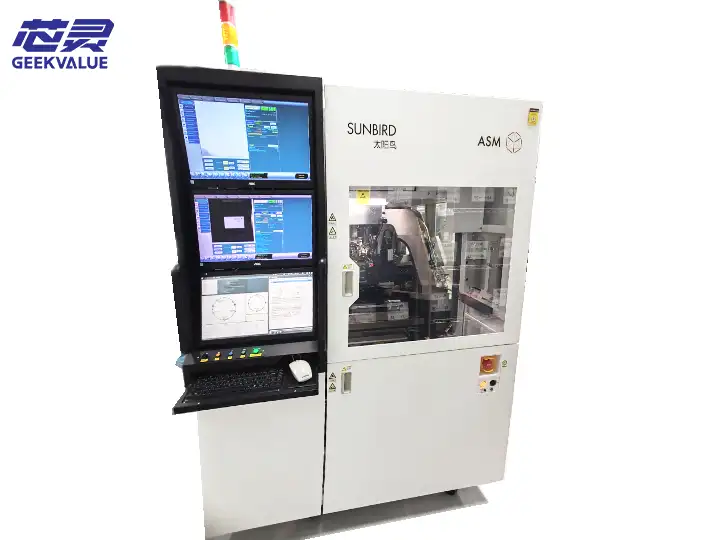
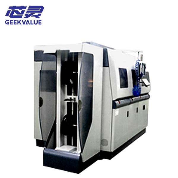
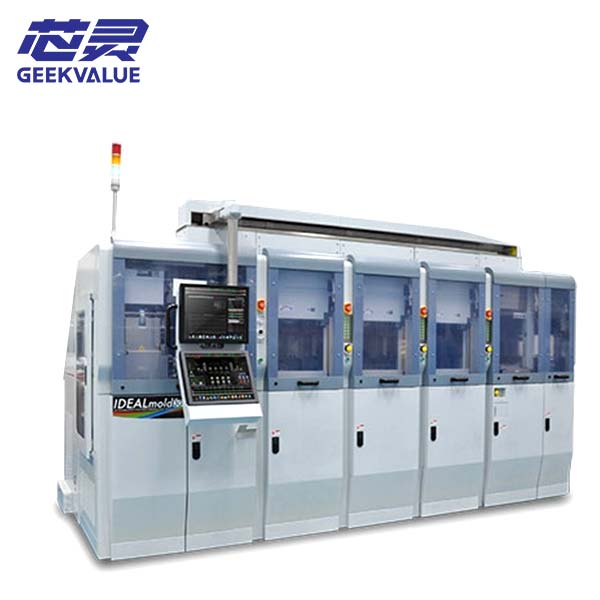
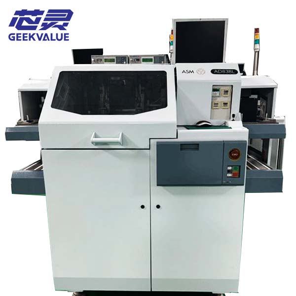
The ASMPT AD832i is a fully automatic multi-process die bonding system designed for semiconductor backend manufacturing environments that require high flexibility, precision, and process integration capability.
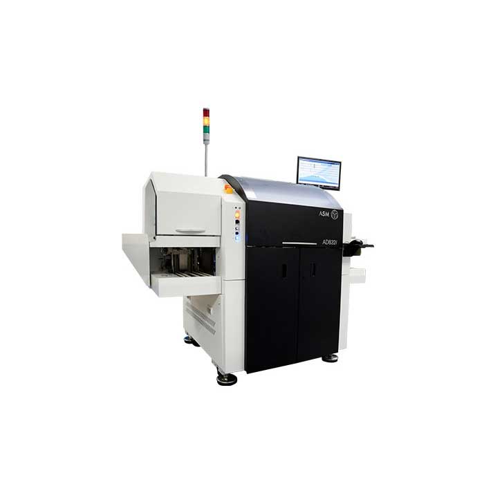
It supports both epoxy die attach and eutectic bonding within a single platform, enabling OSATs and IDMs to efficiently manage high-mix and mid-to-high volume production requirements.
It is widely used in power devices, optoelectronics, and mixed-signal IC manufacturing where rapid process switching and stable placement accuracy are critical to production efficiency.
What is ASMPT AD832i Used For?
The ASMPT AD832i is used for high-precision die attach processes in semiconductor packaging, including epoxy dispensing and metallurgical eutectic bonding.
It places silicon dies onto substrates or leadframes with controlled force, temperature, and alignment, ensuring stable interconnect formation across different material systems.
It is primarily deployed in manufacturing environments requiring flexible process switching between standard packaging and advanced bonding applications.
Industry Applications
The AD832i is widely used across diversified semiconductor packaging segments:
Power Semiconductor Devices
Power MOSFETs requiring thermal-efficient eutectic bonding
IGBT modules for power conversion systems
Power management ICs and discrete devices
Optoelectronics and Sensor Devices
CMOS image sensors requiring precision alignment
MEMS devices with hermetic eutectic sealing requirements
Photodiodes and optical communication components
Mixed-Signal and RF Devices
RF components using AuSn eutectic die attach
Analog and mixed-signal integrated circuits
Standard logic and control ICs in high-mix production lines
Multi-Process Die Bonding in Semiconductor Packaging
Multi-process die bonding refers to a semiconductor assembly capability that integrates epoxy die attach and eutectic bonding within a single automated platform.
This approach allows manufacturers to consolidate different packaging requirements into one system while maintaining process stability, alignment accuracy, and production efficiency.
Competitive Positioning in Die Bonding Equipment Market
The ASMPT AD832i is positioned as a flexible multi-process die bonding platform designed for high-mix semiconductor manufacturing environments.
It is typically selected by manufacturers who need to reduce equipment redundancy while maintaining compatibility with multiple bonding technologies.
Compared to single-process epoxy bonders: supports both epoxy and eutectic bonding with higher application flexibility
Compared to dedicated advanced packaging tools: provides broader process coverage with lower operational complexity
Compared to legacy multi-process systems: improved motion control, vision accuracy, and process repeatability
Technical Capability Overview
Dual-Process Bonding Capability: Supports epoxy dispensing and eutectic bonding within a modular process architecture.
High-Precision Vision Alignment: Enables micron-level placement accuracy for both reflective and standard semiconductor die surfaces.
Force and Temperature Control: Advanced bond head control ensures stable interconnect formation across different bonding materials.
Flexible Material Handling System: Supports multiple wafer sizes, leadframes, and strip-based substrates for high-mix production.
Technical Specifications (Typical Configuration)
| Parameter | Description |
|---|---|
| System Type | Fully automatic multi-process die bonder |
| Placement Accuracy | ±3 μm to ±5 μm @ 3σ (process dependent) |
| Supported Bonding Processes | Epoxy die attach / Eutectic bonding |
| Wafer Size Support | 8-inch / 12-inch (configuration dependent) |
| Substrate Types | Leadframes, laminated substrates, strip carriers |
| Throughput | Variable depending on bonding process and alignment complexity |
Why Manufacturers Use ASMPT AD832i
Consolidates multiple die attach processes into a single equipment platform
Improves production flexibility for high-mix semiconductor manufacturing
Reduces capital equipment investment and factory footprint
Maintains stable process performance across different bonding technologies
Semiconductor Backend Process Flow
Wafer dicing → Die attach (ASMPT AD832i) → Wire bonding → Molding → Singulation → Final testing
Frequently Asked Questions
What is ASMPT AD832i used for?
It is used for multi-process die attach in semiconductor packaging, supporting both epoxy and eutectic bonding for power devices, sensors, and mixed-signal ICs.
Why do manufacturers choose AD832i instead of single-process bonders?
Manufacturers choose the AD832i to improve production flexibility by handling multiple packaging requirements on a single platform, reducing equipment duplication and increasing factory efficiency.
Can AD832i switch between bonding processes easily?
Yes, but switching between epoxy and eutectic processes requires specific bond head modules, tooling kits, and process configuration adjustments.
Summary
The ASMPT AD832i multi-process die bonding system is a flexible semiconductor packaging solution designed for high-mix production environments. It integrates epoxy and eutectic bonding capabilities into a single platform, enabling manufacturers to achieve process consolidation, improved efficiency, and stable production performance.
Request Technical Specification or Quotation
For manufacturers evaluating multi-process die attach equipment, detailed configuration options, tooling specifications, and commercial terms are available upon request.
Equipment specification sheet
Process configuration assessment
Refurbished machine availability
Production line integration support
Email / Inquiry Form Section