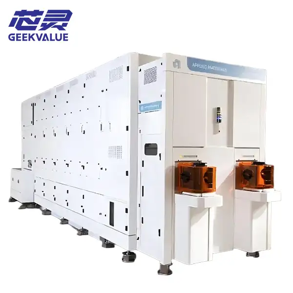
The Applied Materials Raider® Edge ECD is an automated, multi-chamber electrochemical deposition platform developed for single-wafer plating, metal processing and related semiconductor manufacturing applications.
Supporting 150 mm, 200 mm and 300 mm wafer formats, the platform provides manufacturers with the flexibility to process different wafer sizes, substrate types and production requirements on a configurable equipment architecture. Applied Materials describes the Raider Edge ECD as a single-wafer electroplating platform capable of supporting multiple applications, including metal and alloy plating, etching, cleaning and dielectric-layer processing.
Its combination of compact system footprint, high-throughput wafer handling and multi-chamber process capability makes it suitable for semiconductor fabs, advanced packaging facilities, research centers and production lines requiring controlled electrochemical deposition.
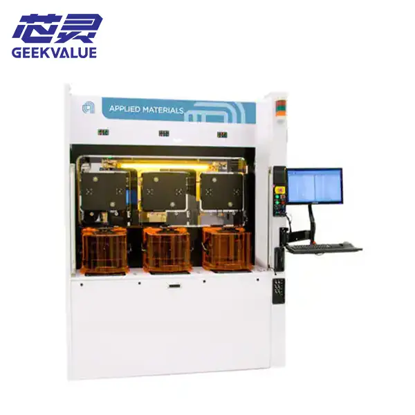
Flexible Electrochemical Processing
The Raider Edge ECD is designed as more than a conventional wafer-plating tool. Depending on its installed process modules and chemical configuration, one platform can support a range of deposition, removal and wafer-cleaning processes.
Potential process functions include:
Electrochemical metal deposition
Single-wafer electroplating
Metal and alloy plating
Electrochemical metal etching
Wafer cleaning
Dielectric-layer etching
Pre-wet and surface-conditioning processes
Post-plating rinsing and drying
The exact process capability of an individual system depends on its chamber configuration, chemical-delivery hardware, wafer-handling setup and installed software.
150 mm, 200 mm and 300 mm Wafer Support
The Applied Materials Raider Edge platform can support 150 mm, 200 mm and 300 mm wafers. This flexibility allows the system to serve established semiconductor processes as well as newer wafer-level and advanced packaging applications.
Before purchasing a used or refurbished system, buyers should confirm:
Installed wafer-size hardware
Wafer carrier and handling configuration
Robot end-effector compatibility
Process chamber compatibility
Software recipes and licenses
Available wafer-size conversion components
A system originally configured for one wafer format may require additional hardware or engineering work before another wafer size can be processed.
Enhanced Electroplating Chamber Technology
For 300 mm wafer electroplating, the Raider ECD platform uses an enhanced chamber reactor capable of dynamically adjusting current density during processing. This design helps improve deposition control and within-wafer uniformity across demanding wafer structures.
Controlled current distribution is particularly important when plating wafers with varying electrical characteristics, feature densities or seed-layer conditions.
Multi-Zone Anode Control
The system incorporates a multi-zone anode-array design intended to improve electroplating performance on ultra-thin and electrically resistive seed layers.
By controlling plating conditions across different wafer regions, the chamber can help address common electrochemical deposition challenges such as:
Center-to-edge thickness variation
Non-uniform current distribution
Resistive seed-layer effects
Pattern-density differences
Wafer-edge process control
Deposition consistency across large wafers
Final performance depends on the process recipe, wafer design, chemistry, chamber condition and installed equipment configuration.
Compact Multi-Chamber Architecture
Raider ECD combines automated wafer handling with a multi-chamber process architecture. Its relatively compact footprint allows multiple process functions to be integrated into one production platform while limiting cleanroom-floor requirements.
Depending on the system configuration, separate chambers may be assigned to different metals, process sequences or wafer-treatment steps.
This architecture may be suitable for:
Engineering development
Process qualification
Pilot production
Mixed-product manufacturing
High-volume wafer processing
Advanced packaging production
Specialty semiconductor applications
High-Throughput Single-Wafer Processing
The platform is designed to provide high production output while processing wafers individually. Single-wafer processing gives manufacturers greater control over recipe execution, wafer tracking and process repeatability than many batch-based plating approaches.
Automated wafer transfer can connect plating, cleaning, etching and drying steps within a coordinated process sequence, reducing manual handling between stages.
Applied Materials also highlights a “teachless” precision-automation design intended to reduce downtime associated with robot reteaching.
Extended Chemistry Management
The Raider ECD uses an ionic membrane intended to help extend the usable life of process chemistry.
Effective chemistry management can help manufacturers control:
Bath stability
Process consistency
Additive consumption
Chemical replacement frequency
Production interruptions
Operating costs
Actual chemical life and process performance will vary according to the deposited material, production volume, bath composition, wafer design and maintenance practices.
Metal Deposition Applications
Electrochemical deposition is widely used to create semiconductor interconnect and packaging structures. Depending on the installed chambers and qualified chemistry, ECD processes can deposit materials such as copper, nickel, gold, silver and tin.
A Raider Edge ECD configuration may therefore be considered for processes involving:
Copper Electroplating
Copper deposition is used in semiconductor interconnects, redistribution structures, pillars, pads and other electrically conductive features.
Wafer-Level Interconnect Formation
Electroplating can form bumps, pillars, redistribution layers and contact pads used in wafer-level packaging and chip interconnection.
Through-Silicon Via Processing
ECD is commonly used to deposit copper into through-silicon vias and similar high-aspect-ratio structures for 2.5D and 3D integration.
Specialty Metal and Alloy Processing
Appropriately configured systems may support additional metals and alloy processes for semiconductor packaging, MEMS, power devices, sensors and specialty components.
The specific supported material must always be verified against the installed process chamber and chemical-delivery configuration.
Advanced Packaging Applications
Electrochemical deposition is an important process in wafer-level and advanced semiconductor packaging. It is used to create structures such as bumps, pillars, redistribution layers, TSVs and contact pads.
Potential applications for a suitably configured Raider Edge ECD include:
Flip-chip packaging
Wafer-level chip-scale packaging
Fan-in wafer-level packaging
Fan-out wafer-level packaging
Copper-pillar formation
Solder-bump processing
Redistribution-layer fabrication
Interposer manufacturing
Through-silicon via processing
2.5D and 3D integration
Hybrid-bonding-related process flows
MEMS and specialty-device manufacturing
Main Equipment Advantages
Supports 150 mm, 200 mm and 300 mm wafers
Automated single-wafer processing
Multi-chamber process architecture
Compact cleanroom footprint
High-throughput wafer handling
Plating and etching capability
Supports multiple substrate types and thicknesses
Enhanced current-density control
Multi-zone anode-array technology
Designed for thin and resistive seed layers
Integrated wafer cleaning capabilities
Suitable for multiple process applications
Teachless precision automation
Scalable for engineering and production use
Typical System Configuration
An Applied Materials Raider Edge ECD system may include different combinations of:
Electroplating process chambers
Metal-etching chambers
Wafer-cleaning modules
Dielectric-etching modules
Pre-wet chambers
Spin-rinse-dry modules
Chemical-delivery systems
Chemistry tanks and filtration units
Automated wafer-transfer robots
Wafer aligners
Load ports
Factory interface modules
Process-control software
Facilities and exhaust components
Because systems are often configured for a specific production process, chamber quantity and functionality may vary significantly between available units.
Information to Confirm Before Purchase
When evaluating a used Applied Materials Raider Edge ECD, buyers should not rely only on the model designation. The complete installed configuration should be inspected and verified.
Important items include:
Equipment manufacturing year
Current operational condition
Supported wafer size
Number and type of process chambers
Supported plating metals
Supported etching processes
Chemical-delivery configuration
Chamber and anode condition
Wafer-robot condition
Software version
Recipe availability
Maintenance history
Facility requirements
Included accessories
Available spare parts
Deinstallation status
Packaging and shipping scope
This information determines whether the system can be introduced directly into the intended process or requires refurbishment, reconfiguration or chamber conversion.
Available Equipment and Services
Available Raider Edge ECD configurations may vary according to inventory. Equipment information can include system photos, manufacturing year, wafer-size configuration, chamber layout, condition information and included modules.
Project services may include:
Semiconductor equipment sourcing
System-configuration verification
Equipment inspection
Refurbishment coordination
Deinstallation support
Export packing
International transportation
Installation coordination
Spare-parts sourcing
Technical consultation
Customers should provide their required wafer size, plating metal, process application, chamber configuration and destination country so that the available equipment can be evaluated against the project requirements.
Why Choose the Applied Materials Raider Edge ECD?
The Raider Edge ECD is suitable for manufacturers seeking a flexible single-wafer electrochemical processing platform rather than a fixed-purpose plating machine.
Its ability to combine metal deposition, etching, cleaning and related wafer-processing functions on one automated multi-chamber platform helps production facilities support changing process requirements while controlling cleanroom space.
Support for multiple wafer sizes, substrate types and process applications also makes the platform relevant to both established semiconductor manufacturing and advanced packaging development.
Frequently Asked Questions
What is the Applied Materials Raider Edge ECD?
It is an automated, multi-chamber electrochemical deposition platform designed for single-wafer electroplating and related wafer-processing applications.
Which wafer sizes does Raider Edge ECD support?
The platform supports 150 mm, 200 mm and 300 mm wafers. The actual capability of an available system depends on its installed wafer-handling and chamber hardware.
Is Raider Edge ECD only used for electroplating?
No. Depending on its configuration, the platform can perform metal and alloy plating, metal etching, wafer cleaning and dielectric-layer etching.
Can the system process different substrate types?
Yes. Applied Materials states that Raider Edge can work with multiple substrate types and thicknesses, although compatibility must be verified for the individual system configuration.
Is Raider Edge suitable for advanced packaging?
Yes. Electrochemical deposition is used in advanced packaging applications such as bumps, copper pillars, redistribution layers, TSVs, contact pads, fan-out packaging and 2.5D or 3D integration.
What should be checked when buying a used Raider Edge ECD?
Buyers should confirm wafer size, chamber configuration, supported metals and chemicals, automation condition, software version, facility requirements, maintenance history and included accessories.
Request Raider Edge ECD Equipment Information
Looking for an Applied Materials Raider® Edge ECD system?
Send us your required wafer size, plating or etching process, target material, preferred chamber configuration, equipment condition and destination country. We will review the available equipment and provide relevant system details, photos, configuration information and quotation.