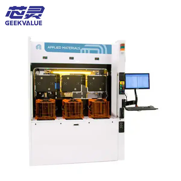
The Applied Materials Nokota™ ECD is a production-oriented electrochemical deposition platform developed for advanced semiconductor packaging and wafer-level plating processes.
Designed to combine wafer protection, process flexibility and scalable chamber configuration, the system can support manufacturers working with multiple packaging technologies, wafer formats and metal deposition requirements. It is suitable for semiconductor manufacturers, foundries, research facilities and outsourced semiconductor assembly and test companies seeking an adaptable electroplating platform for development or volume production.
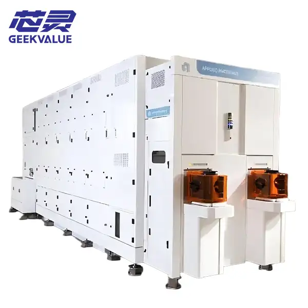
Nokota ECD can be used for plating processes associated with flip-chip packaging, wafer-level chip-scale packaging, fan-out packaging, interposers, through-silicon vias and other advanced interconnect structures. ble Electroplating for Advanced Semiconductor Packaging
Modern packaging facilities often need to process different device structures, metal stacks and wafer sizes on the same production floor. The Nokota platform addresses this requirement through a modular system architecture that can be configured around specific production objectives.
Depending on the installed chamber and chemical delivery configuration, the system can support commonly used plating metals such as:
Copper
Tin-silver alloy
Nickel
Gold
Tin
Palladium
Other application-specific plating materials
Applied Materials states that the platform can support 150 mm, 200 mm and 300 mm wafer processing, including mixed wafer-size configurations such as 150/200 mm and 200/300 mm operation. eatures of the Applied Materials Nokota ECD
Advanced Wafer Protection
The Nokota platform incorporates Applied Materials SafeSeal™ wafer protection technology. The wafer is sealed before plating and remains protected throughout single-metal or multi-metal process sequences.
Seal verification, post-process cleaning and inspection functions help reduce the risk of plating chemistry reaching sensitive wafer areas. This is especially important for high-value wafers and complex packaging structures requiring multiple deposition steps. wap™ Seal Maintenance
The HotSwap™ design allows SafeSeal components to be serviced outside the active process chamber. Seal replacement and maintenance can therefore be performed without requiring the complete plating platform to stop processing.
This architecture is intended to reduce unplanned production interruptions and support higher equipment availability in manufacturing environments. ™ Process Chamber
The VMax™ process chamber is designed to improve mass-transfer control during electrochemical deposition. It supports high plating rates while maintaining the coplanarity and within-wafer consistency required by advanced packaging structures.
Integrated chamber cleaning allows the wafer to be rinsed immediately following the plating process, helping control chemical carryover and maintain process cleanliness. lar Chamber Configuration
Unlike platforms that require process chambers to be installed only in fixed pairs, the Nokota system supports individual chamber configuration.
This provides greater flexibility when building a system for:
Process development
Engineering qualification
Pilot production
Mixed-product manufacturing
High-volume semiconductor packaging
The platform can be expanded or reconfigured as production requirements change, allowing users to balance initial equipment investment with future capacity needs. onductor Packaging Applications
The Applied Materials Nokota ECD system can be considered for a broad range of wafer-level and advanced packaging applications, including:
Copper Pillar and Bump Plating
The system can be configured for copper pillar, solder bump and related interconnect plating processes used in flip-chip and high-density packaging.
Wafer-Level Chip-Scale Packaging
Nokota supports electroplating steps used in wafer-level chip-scale packages where compact dimensions, electrical performance and controlled interconnect formation are required.
Fan-Out Wafer-Level Packaging
The platform is suitable for metal deposition processes associated with 2D and 3D fan-out structures, including redistribution-layer and interconnect applications.
Through-Silicon Via Processing
Copper and other metal deposition configurations can be used for through-silicon via and interposer-related processes where controlled feature filling and deposition uniformity are important.
2.5D and 3D Integration
The system supports plating requirements used in interposer-based packages and other advanced integration schemes for high-performance computing, communication, sensor, power-device and automation applications. System Advantages
Supports multiple advanced packaging applications
Compatible with several commonly used plating metals
Available for 150 mm, 200 mm and 300 mm wafer processing
Supports mixed wafer-size production configurations
Modular process chamber architecture
Automated wafer sealing and protection
Seal inspection and verification functions
Integrated post-plating wafer rinsing
Scalable for development, pilot and volume production
Suitable for single-metal and multi-metal plating sequences
Flexible configuration for mixed-product manufacturing
Typical Process Capabilities
The exact process capability of an individual Nokota ECD system depends on its installed hardware, chamber types, chemical tanks, wafer-handling modules and software configuration.
A system may include combinations of:
Electrochemical plating chambers
Copper plating modules
Tin-silver plating modules
Nickel or other metal plating modules
Vacuum pre-wet chambers
Spin-rinse-dry modules
Seal-ring maintenance stations
Chemical delivery and management systems
Wafer handling and transfer modules
Wafer-size bridge or conversion hardware
Before purchasing a used or refurbished Nokota system, buyers should verify the chamber count, supported chemistries, wafer-size configuration, facility requirements, software revision and included accessories.
Available Equipment Information
Please contact us with your required process and production specifications. To identify a suitable Applied Materials Nokota ECD configuration, provide the following information:
Required wafer size
Target plating metal
Intended packaging process
Required number of process chambers
Development or production application
Preferred equipment condition
Installation country
Required delivery schedule
Available system specifications, manufacturing year, chamber layout and included modules may vary according to current inventory.
Equipment Inspection and Technical Support
Before shipment, available equipment can be evaluated according to the condition and scope of the individual system. Inspection may include verification of major modules, chamber configuration, wafer-handling components, chemical delivery hardware and included accessories.
Additional services may be discussed according to project requirements, including:
Equipment sourcing
Configuration verification
On-site or remote inspection
Deinstallation coordination
Export packing
International transportation
Installation support
Spare-parts sourcing
Technical consultation
Why Choose the Applied Materials Nokota ECD?
The Nokota ECD is designed for semiconductor manufacturers that require more than a conventional single-process plating tool.
Its combination of modular chamber configuration, multi-metal capability, wafer protection technology and support for multiple wafer formats makes it particularly suitable for advanced packaging operations with changing product mixes.
For facilities moving from engineering development into production, the platform provides a path to expand process capacity without replacing the complete equipment architecture.
Frequently Asked Questions
What is the Applied Materials Nokota ECD used for?
The Nokota ECD is an electrochemical deposition system used for metal plating processes in wafer-level and advanced semiconductor packaging. Typical applications include bumps, copper pillars, redistribution structures, fan-out packaging, interposers and through-silicon vias.
Which wafer sizes can the Nokota ECD process?
The platform can support 150 mm, 200 mm and 300 mm wafer processing. The actual wafer-size capability of a specific system must be confirmed from its installed hardware and configuration. h metals can be plated on the Nokota system?
Depending on the installed process chambers and chemical systems, the platform can support copper, tin-silver, nickel, gold, tin, palladium and other plating materials. one system support multiple plating metals?
Yes. Nokota is designed to support both single-metal and multi-metal plating sequences. The exact number and type of metals depend on the chamber and chemical-delivery configuration.
Is the system suitable for advanced packaging production?
Yes. The platform was developed for wafer-level and advanced packaging applications, including flip chip, fan-out, wafer-level chip-scale packaging, interposers and TSV-related processes. should be checked before purchasing a used Nokota ECD?
Important items include the system manufacturing year, operational status, wafer size, chamber quantity, supported plating metals, chemical tank configuration, software version, maintenance history, facility requirements and included spare parts.
Request Applied Materials Nokota ECD Information
Looking for an Applied Materials Nokota™ ECD electrochemical deposition system?
Send us your required wafer size, plating process, metal type, chamber configuration and destination country. Our equipment team will review the available system configuration and provide equipment details, photos, condition information and a quotation based on your project requirements.