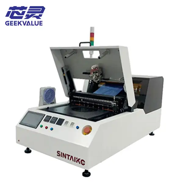
The SINTAIKE STK-7080 semiconductor wafer mounter is an advanced wafer tape lamination system designed for thin wafer and compound semiconductor processing applications. Unlike traditional roller-based wafer mounting equipment, the STK-7080 adopts non-contact vacuum lamination technology to reduce mechanical stress and protect fragile wafers during semiconductor manufacturing.
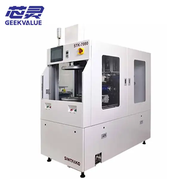
As semiconductor devices become thinner and more sensitive, conventional tape mounting methods may create risks such as wafer cracking, surface damage, and uneven adhesion. The SINTAIKE STK-7080 addresses these challenges through vacuum-based film application technology, providing a stable solution for next-generation wafer processing requirements.
The system is particularly suitable for advanced materials including silicon carbide (SiC), gallium nitride (GaN), gallium arsenide (GaAs), and thin silicon wafers. :contentReference[oaicite:1]{index=1}
What is SINTAIKE STK-7080 Wafer Mounter?
The SINTAIKE STK-7080 is a semi-automatic non-contact vacuum wafer mounting machine used for semiconductor wafer protection tape application before dicing or other backend processes.
The primary function of the equipment is to attach blue film or UV film onto wafer surfaces while minimizing physical pressure during lamination.
Traditional wafer mounting systems often use rollers to press adhesive film onto wafers. However, thin and fragile wafers may suffer from mechanical stress during this process. The STK-7080 replaces direct roller contact with vacuum lamination technology, improving wafer safety and process stability.
Why Non-Contact Vacuum Lamination is Important
Modern semiconductor manufacturing increasingly requires thinner wafers and more fragile materials. Advanced devices such as SiC power semiconductors and compound semiconductor wafers require careful handling throughout backend processes.
The non-contact vacuum mounting method provides several advantages:
Reduce mechanical pressure on fragile wafers
Minimize wafer cracking risk
Improve tape adhesion uniformity
Reduce bubble formation during lamination
Support advanced semiconductor materials
Key Features of SINTAIKE STK-7080 Wafer Mounter
Non-Contact Vacuum Lamination Technology
The biggest difference between STK-7080 and conventional wafer mounters is its roller-free vacuum lamination technology.
Instead of applying mechanical pressure directly through rollers, the system uses controlled vacuum pressure to attach adhesive film onto the wafer surface. This approach helps protect thin wafers from stress and scratches.
Designed for Thin and Fragile Wafers
The STK-7080 is optimized for applications where wafer strength is limited. It supports thin wafer processing with thickness ranges from approximately 100μm to 750μm depending on process requirements. :contentReference[oaicite:2]{index=2}
Typical applications include:
Thin silicon wafers
SiC power semiconductor wafers
GaAs compound semiconductor wafers
GaN semiconductor wafers
MEMS wafer applications
Automatic Film Feeding and Cutting
The system integrates automatic film feeding, lamination, circular cutting, waste film collection, and release liner collection functions.
This reduces manual operation requirements and improves process consistency in semiconductor production environments. :contentReference[oaicite:3]{index=3}
Blue Film and UV Film Compatibility
The STK-7080 supports semiconductor wafer films including blue film and UV film, providing flexibility for different dicing and wafer handling processes.
Anti-Static Protection
Static control is important when processing semiconductor materials. The STK-7080 integrates ionizing air systems to reduce electrostatic risks during wafer mounting. :contentReference[oaicite:4]{index=4}
SINTAIKE STK-7080 Technical Specifications
| Parameter | Description |
|---|---|
| Equipment Type | Non-contact vacuum wafer mounter |
| Manufacturer | SINTAIKE |
| Technology | Roller-free vacuum lamination |
| Wafer Size | 4 inch - 8 inch wafer |
| Wafer Material | Silicon, SiC, GaAs, GaN |
| Wafer Thickness | 100μm - 750μm |
| Film Type | Blue film / UV film |
| Position Accuracy | Approximately ±0.5mm |
| Control System | PLC control with touchscreen interface |
| Operation Mode | Semi-automatic |
Specifications may vary depending on equipment configuration and customer process requirements. :contentReference[oaicite:5]{index=5}
SINTAIKE STK-7080 Wafer Mounting Process Flow
Wafer preparation
Film loading
Wafer positioning
Vacuum lamination
Film cutting
Inspection and transfer
Dicing or downstream wafer process
Process Flow:
Wafer Preparation → Film Loading → Vacuum Mounting → Inspection → Wafer Dicing
Applications of SINTAIKE STK-7080
Compound Semiconductor Manufacturing
The STK-7080 is suitable for compound semiconductor materials including SiC, GaN, and GaAs where wafer protection is critical.
Power Semiconductor Processing
Power semiconductor manufacturers increasingly use fragile materials requiring advanced wafer handling technologies.
Thin Wafer Processing
Ultra-thin wafers require low-stress mounting solutions to reduce breakage during backend manufacturing.
MEMS and Sensor Manufacturing
MEMS wafers often contain sensitive structures that require careful mechanical handling during processing.