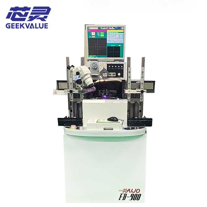
The KAIJO FB-e20N is a fully automatic thermosonic wire bonder designed for high-volume semiconductor backend manufacturing. It is optimized for mainstream integrated circuits and discrete power devices, where stable process windows, high throughput (UPH), and low total cost of ownership (TCO) are critical manufacturing requirements.
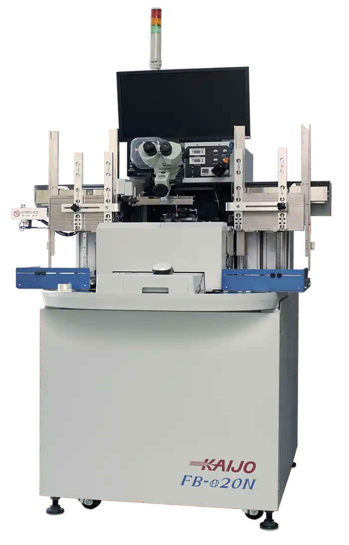
The system is widely deployed in OSAT and IDM production lines for consumer electronics, power semiconductors, and standard logic packages, supporting the ongoing transition from gold (Au) wire to copper (Cu) and palladium-coated copper (PCC) wire processes.
1. System Overview & Manufacturing Positioning
The FB-e20N is positioned as a mainstream wire bonding platform placed after die attach in the backend assembly flow. It prioritizes mechanical robustness, process stability, and wide manufacturing tolerance windows over ultra-fine-pitch capability.
Its architecture is optimized for long-run production stability, reducing downtime, maintenance frequency, and operator intervention in high-volume manufacturing environments.
2. Thermosonic Bonding Process & Wire Compatibility
The system supports thermosonic bonding, which combines ultrasonic energy, heat, and mechanical force to form reliable intermetallic compound (IMC) connections at both ball bond and stitch bond interfaces.
EFO (Electronic Flame-Off) Control: Ensures stable Free Air Ball (FAB) formation with controlled spark energy, critical for repeatable first-bond quality.
Copper Wire Process Adaptation: Compensates for higher oxidation sensitivity and mechanical hardness of Cu and PCC wires through optimized energy profiles.
Forming Gas Compatibility: Supports inert/reducing environments to improve copper wire bonding stability and reduce oxide formation.
3. Vision Alignment & Process Yield Control
A high-speed Pattern Recognition System (PRS) is integrated to ensure stable alignment accuracy under high-UPH conditions. The system detects leadframe or substrate fiducials and compensates for mechanical indexing errors and material deformation.
This enables precise capillary positioning within pad openings, maintaining consistent bond yield in standard-pitch semiconductor packages.
4. Target Application Ecosystem
The FB-e20N is optimized for mature semiconductor packaging segments requiring high throughput and cost efficiency:
Power Semiconductor Devices
Power MOSFETs
Rectifiers and diodes
General-purpose power management ICs
Consumer & Industrial ICs
Microcontrollers (MCUs)
Analog ICs and interface chips
Home appliance control modules
Standard Memory Packages
DRAM and NAND flash packaging
5. Technical Specifications (Typical Configuration)
| Parameter | Specification |
|---|---|
| System Type | Fully automatic thermosonic wire bonder |
| Supported Wire Materials | Gold (Au), Copper (Cu), Palladium-Coated Copper (PCC) |
| Bonding Accuracy | ±2.0 μm to ±3.5 μm @ 3σ (process dependent) |
| Wire Diameter Range | 15 μm – 50 μm |
| Substrate Types | Leadframes, organic laminates, strip carriers |
| Production Focus | High-volume manufacturing (high UPH / stable yield) |
6. Backend Packaging Process Flow
The FB-e20N operates as the electrical interconnect formation step in semiconductor backend assembly:
Wafer dicing → Die attach (epoxy / sintering) → Wire bonding (FB-e20N) → Molding / Encapsulation → Singulation → Final electrical test
7. Engineering Evaluation & Manufacturing Economics
7.1 Cost-of-Ownership Optimization
The platform is designed for low total cost of ownership (TCO), featuring simplified maintenance architecture, stable long-term operation, and reduced process tuning complexity for high-volume production lines.
7.2 Copper Wire Transition Capability
The system supports copper (Cu) and palladium-coated copper (PCC) wire bonding through optimized EFO energy control and forming gas process compatibility, improving manufacturability during industry-wide material transition.
7.3 Process Limitations
The FB-e20N is not optimized for ultra-fine-pitch applications (<40 μm) or advanced stacked-die architectures requiring complex loop control. These applications require advanced wire bonders with higher precision motion systems and enhanced loop trajectory control.
8. Summary
The KAIJO FB-e20N wire bonder provides a robust and cost-efficient solution for high-volume semiconductor manufacturing. It delivers stable thermosonic bonding performance, strong copper wire process compatibility, and reliable throughput for mainstream logic, memory, and power semiconductor packaging applications.
9. Request Technical Specification or Quotation
For engineering evaluation of wire bonding equipment, detailed machine specifications, process compatibility matrices, and production line integration guidance are available upon request.
Equipment specification sheet
Gold vs Copper wire process analysis
System configuration options
Production line integration consulting
Contact engineering team for technical support or quotation.