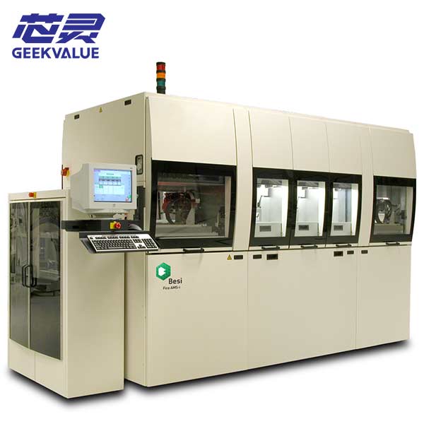
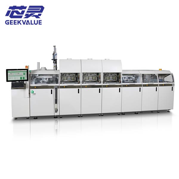
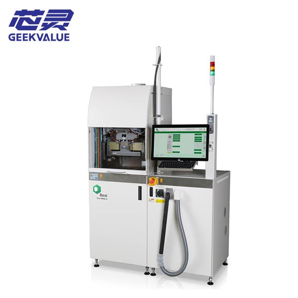
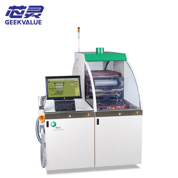
The transition from wire bonding to flip chip architectures in mainstream semiconductor packaging introduces a critical manufacturing challenge: maintaining high throughput while managing the complexities of fine-pitch interconnects. The BESI Esec 2100 FC hS addresses this by combining high-speed die handling with the precision required for mass reflow flip chip assembly.
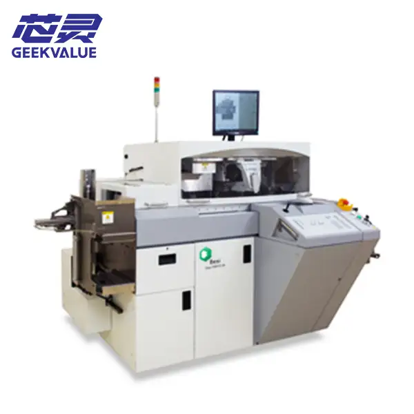
It is deployed by OSATs and IDMs scaling up flip chip production for mobile processors, RF devices, and high-density memory packages where units-per-hour (UPH) directly impacts cost-of-ownership.
Phi-Y Motion Architecture and Throughput Dynamics
The core differentiator of the Esec 2100 FC hS is its proprietary Phi-Y motion concept. Unlike traditional linear X-Y gantry systems, this platform utilizes a combination of rotational (Phi) and linear (Y-axis) movement.
This architecture significantly reduces the travel distance and idle time between the wafer pickup position and the substrate placement position. By minimizing mechanical transition times, the system achieves throughput rates up to 16,000 UPH, making it one of the fastest flip chip bonders in its accuracy class.
8μm Alignment and Process Control
While prioritizing speed, the platform maintains the alignment tolerances required for modern flip chip interconnects. The system is engineered to deliver a placement accuracy of 8 μm @ 3σ under typical production conditions.
This level of precision is supported by:
High-Resolution Vision Processing: Simultaneous pattern recognition of die bumps and substrate pads to correct for positional offset and localized substrate distortion.
Dynamic Bond Force Regulation: Closed-loop control of the bond head ensures consistent pressure across the die surface during placement, preventing micro-bump damage or collapse prior to reflow.
Integrated Flux Management: Precision flux dipping or dispensing modules ensure uniform bump coverage, which is critical for yield reliability during subsequent mass reflow processes.
High-Volume Flip Chip Workflow Integration
The Esec 2100 FC hS is positioned as a mass production tool within the advanced packaging backend flow. It handles bare bumped dies directly from wafer ring frames and places them onto organic laminates or leadframes.
The typical process integration sequence is structured for continuous production:
Wafer bumping → Wafer dicing → Flux application (dip/dispense) → High-speed flip chip placement (Esec 2100 FC hS) → Mass reflow → Underfill dispensing → Curing → Final electrical testing
Equipment Specifications and Engineering Parameters
Actual performance parameters are highly dependent on die geometry, bump layout, and substrate material composition.
| Parameter | Engineering Specification |
|---|---|
| Platform Classification | Fully automatic high-speed flip chip bonder |
| Placement Accuracy | 8 μm @ 3σ (process and tooling dependent) |
| Maximum Throughput | Up to 16,000 UPH (optimized for mass reflow applications) |
| Motion Architecture | Phi-Y (rotational and linear combined) |
| Bonding Methodology | Mass reflow (post-placement) |
| Substrate Compatibility | Organic laminates, leadframes, strip-based carriers |
Engineering Evaluation
How does the Phi-Y concept improve flip chip throughput?
By replacing standard orthogonal X-Y movements with a rotational pivot, the die travels via the shortest physical path from the wafer to the substrate. This reduces mechanical settling times and allows the bond head to operate at higher accelerations without inducing vibration.
Is the 8μm accuracy sufficient for advanced 5G and AI packaging?
It is suitable for mainstream flip chip pitches (typically >100μm). For sub-40μm micro-bump interconnects required in 2.5D/3D heterogeneous integration, ultra-precision thermocompression bonding (TCB) equipment with sub-micron accuracy is required instead.
What types of flux systems are compatible?
The platform is designed for high-volume mass reflow, meaning it utilizes integrated flux dipping trays or precision jet dispensing modules to apply solder flux immediately prior to die placement, ensuring reliable joint formation during the off-line reflow oven process.
Summary
The BESI Esec 2100 FC hS provides a high-throughput pathway for semiconductor manufacturers transitioning to flip chip interconnects. By leveraging the proprietary Phi-Y motion architecture and maintaining 8μm placement accuracy, it balances the production speed of traditional die bonders with the process control required for reliable mass reflow flip chip packaging.
Request Technical Specification or Quotation
For engineering teams evaluating high-speed flip chip assembly equipment, detailed machine specifications, flux module configurations, and process compatibility reports are available upon request.
Detailed equipment specification sheet
Process compatibility assessment for specific bump pitches
System configuration options
Production line integration consulting
Contact engineering team for technical evaluation or quotation support.