The SCREEN SU-3200 wafer cleaner is a high-throughput 300mm single wafer cleaning system developed by SCREEN Semiconductor Solutions for advanced semiconductor manufacturing. It is designed to provide stable wafer processing, flexible chemical delivery, and efficient production capacity in high-volume fabrication environments.
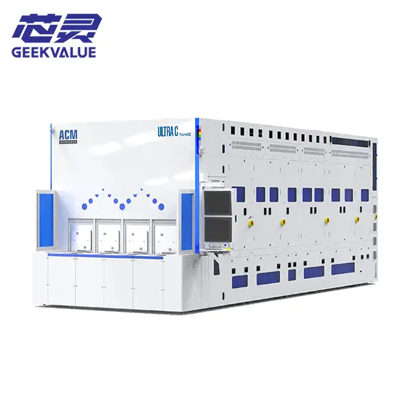
As semiconductor structures become smaller and more complex, wafer cleaning equipment must remove particles, chemical residues, organic contamination, and process by-products without damaging sensitive wafer patterns. The SCREEN SU-3200 combines multi-chamber processing, controlled wafer handling, and configurable cleaning technology for demanding front-end semiconductor processes.
What Is the SCREEN SU-3200 Wafer Cleaner?
The SCREEN SU-3200 is a single wafer wet cleaning system used in semiconductor front-end fabrication. It processes wafers individually, allowing the cleaning recipe, chemical delivery, rinse sequence, drying conditions, and process time to be controlled for each wafer.
Compared with batch cleaning systems that process multiple wafers in the same tank, single wafer cleaning provides greater flexibility for advanced processes and helps reduce the risk of cross-contamination between wafers.
The SU-3200 is designed for 300mm wafer production and can be configured with multiple process chambers. Depending on the installed configuration and process recipe, the system may support up to 12 chambers and throughput of up to 800 wafers per hour.
Actual production capacity depends on the cleaning process, chamber arrangement, chemical sequence, wafer handling conditions, drying requirements, and equipment configuration.
Why Wafer Cleaning Is Critical in Semiconductor Manufacturing
Semiconductor wafers pass through many deposition, lithography, etching, implantation, stripping, and polishing processes. Each production step can leave unwanted contamination on the wafer surface.
Common wafer contaminants include:
Particles and airborne contamination
Photoresist and organic residues
Metal contamination
Chemical residues
Etching by-products
Post-CMP slurry residues
Moisture and drying marks
If these contaminants are not properly removed, they may cause pattern defects, poor film adhesion, electrical leakage, yield loss, and long-term device reliability problems.
A properly configured wafer cleaning system helps maintain surface cleanliness before the wafer moves to the next semiconductor fabrication process.
Key Technologies of the SCREEN SU-3200
High-Throughput Single Wafer Processing
The SCREEN SU-3200 is designed for high-volume 300mm wafer production. Its multi-chamber architecture allows different cleaning, rinsing, and drying processes to operate in parallel.
The system can be configured with up to 12 process chambers, depending on the required production setup. This chamber arrangement helps increase processing capacity while controlling the overall equipment footprint.
Up to 800 Wafers per Hour
Depending on the process recipe and system configuration, the SU-3200 can provide throughput of up to 800 wafers per hour.
The actual throughput achieved in production depends on chamber quantity, chemical processing time, rinse and drying requirements, wafer transfer speed, and recipe complexity.
APAC Process Atmosphere Control
The SU-3200 incorporates SCREEN process atmosphere control technology designed to manage the environment around the wafer during processing.
Controlled airflow and chamber conditions help reduce contamination exposure and support stable wafer processing. The installed chamber technology and available functions should be confirmed for each individual system.
Controlled Wafer Drying
Drying is an important stage of the wafer cleaning process because remaining moisture or drying marks may affect subsequent fabrication steps.
The SU-3200 uses controlled drying technology designed to reduce watermark formation and provide repeatable post-clean surface conditions.
Flexible Chemical Supply Configuration
The equipment may be configured with different chemical delivery arrangements according to the required production process.
Available configurations can include Dynamic Direct Injection and cabinet-based chemical supply systems. Compatibility depends on the installed chemical modules, facilities, process chambers, and recipe requirements.
Automatic Wafer Handling
The wafer transfer system automatically moves wafers between the load ports, transfer area, process chambers, and output position.
Accurate wafer handling is important for preventing wafer damage, transfer errors, particle generation, and production interruptions.
Recipe-Based Process Control
Cleaning parameters can be managed through stored process recipes. Depending on the equipment configuration, adjustable parameters may include chemical selection, chemical flow, process time, rinse sequence, wafer rotation, temperature, and drying conditions.
SCREEN SU-3200 Technical Information
| Parameter | Description |
|---|---|
| Manufacturer | SCREEN Semiconductor Solutions |
| Model | SU-3200 |
| Equipment Type | Single wafer wet cleaning system |
| Wafer Size | 300mm |
| Processing Method | Single wafer cleaning, rinsing, and drying |
| Maximum Chamber Configuration | Up to 12 process chambers, depending on configuration |
| Maximum Throughput | Up to 800 wafers per hour, depending on process conditions |
| Wafer Handling | Automatic wafer loading, transfer, processing, and unloading |
| Chemical Supply | Configuration-dependent chemical delivery system |
| Process Control | Programmable cleaning, rinsing, chemical supply, and drying recipes |
| Main Applications | Advanced logic, memory, post-etch, post-strip, and related wafer cleaning processes |
Exact specifications may vary according to the machine production year, hardware configuration, chamber quantity, chemical modules, software version, factory options, and previous application.
The equipment nameplate, configuration list, facility requirements, and current operating condition should be verified before purchase.
Applications of the SCREEN SU-3200 Wafer Cleaner
Advanced Logic Device Manufacturing
Advanced logic devices require strict control of particles, residues, and metallic contamination. The SU-3200 can be configured for cleaning processes used between critical semiconductor fabrication steps.
Memory Semiconductor Production
DRAM, NAND flash, and other memory products use complex structures and repeated fabrication processes. Stable wafer cleaning helps maintain surface conditions and reduce contamination-related defects.
Post-Etch Cleaning
Plasma etching may leave polymer residues and other process by-products on the wafer surface. A suitable cleaning recipe is required to remove these residues before the next deposition or patterning process.
Post-Photoresist Strip Cleaning
After photoresist removal, remaining organic material and process residues may require additional wet cleaning. The SU-3200 can be configured according to the required chemical sequence and wafer surface conditions.
Post-CMP Cleaning
Chemical mechanical planarization may leave slurry particles, polishing residues, and metallic contamination on the wafer. The appropriate process module and recipe are required for post-CMP applications.
Pre-Deposition Surface Preparation
Before deposition or other critical fabrication steps, wafers may require controlled surface preparation to remove contamination and provide suitable surface conditions.
SCREEN SU-3200 Wafer Cleaning Process
Load the wafer carrier or front-opening unified pod into the equipment.
Identify the wafer lot and select the required cleaning recipe.
Transfer the wafer from the load port to the assigned process chamber.
Apply the specified chemical cleaning sequence.
Remove particles, organic residues, metallic contamination, or process by-products.
Rinse the wafer using deionized water or the specified rinse process.
Dry the wafer under controlled process conditions.
Return the processed wafer to the designated output position.
Transfer the wafer lot to the next semiconductor fabrication process.
Typical process flow:
Wafer Loading → Recipe Selection → Chamber Transfer → Chemical Cleaning → DI Water Rinse → Controlled Drying → Wafer Unloading
Advantages of the SCREEN SU-3200
Designed for 300mm single wafer processing
Multi-chamber configuration for high-volume production
Throughput of up to 800 wafers per hour, depending on process conditions
Configurable chemical cleaning, rinsing, and drying processes
Automatic wafer loading and transfer
Recipe-based process control
Suitable for advanced logic and memory fabrication environments
Flexible chamber and chemical supply configuration
Important Points When Selecting a Used SCREEN SU-3200
A used SCREEN SU-3200 should be evaluated according to its complete configuration and current operating condition. The model name alone does not confirm that the machine is suitable for a specific cleaning process.
Important inspection points include:
Complete model, serial number, and manufacturing information
Number and type of installed process chambers
Previous chemical and production applications
Chemical supply cabinet and delivery-line condition
Process chamber, nozzle, spin motor, and exhaust condition
Robot, aligner, load port, and wafer transfer accuracy
Drying system and contamination-control performance
Control computer, software version, recipes, and backup files
Utility requirements, including power, exhaust, water, chemicals, and compressed air
Availability of manuals, accessories, spare parts, and maintenance records
When possible, the machine should undergo a power-on inspection, wafer transfer test, chamber operation test, alarm check, and process-function verification before shipment.
SCREEN SU-3200 Maintenance Considerations
Regular inspection and preventive maintenance are necessary to maintain stable wafer handling, chemical delivery, particle control, and cleaning repeatability.
Inspect chemical supply lines, valves, pumps, filters, and flow-control components.
Clean and inspect process chambers according to the maintenance schedule.
Check spray nozzles, chemical outlets, and wafer spin components.
Monitor wafer transfer accuracy and robot positioning.
Inspect the drying system and verify post-clean wafer condition.
Monitor particle performance and process repeatability.
Verify process recipes after hardware replacement or maintenance.
Check exhaust, leakage detection, interlocks, and other safety systems.
Maintenance procedures should be carried out by trained personnel using appropriate safety controls, especially when inspecting chemical delivery and wet process components.
SCREEN SU-3200 Equipment Supply and Configuration Support
We supply selected SCREEN SU-3200 wafer cleaning systems for semiconductor manufacturing, process expansion, and equipment replacement projects.
The chamber configuration, chemical modules, wafer handling system, software, accessories, documentation, refurbishment scope, and delivery condition may vary between individual machines.
To confirm whether an available SCREEN SU-3200 matches your process, please provide the required wafer size, cleaning application, chemical process, target throughput, chamber requirements, factory utilities, destination country, and preferred equipment condition.