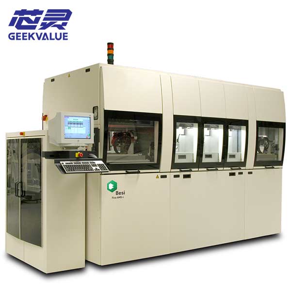
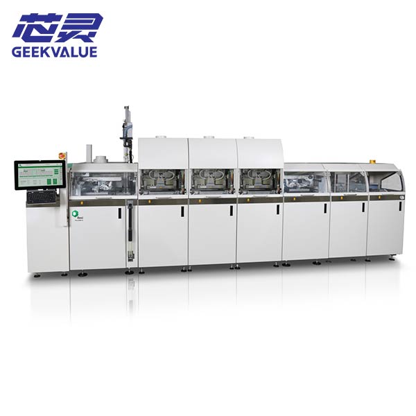
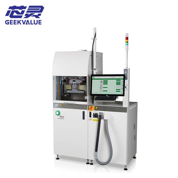
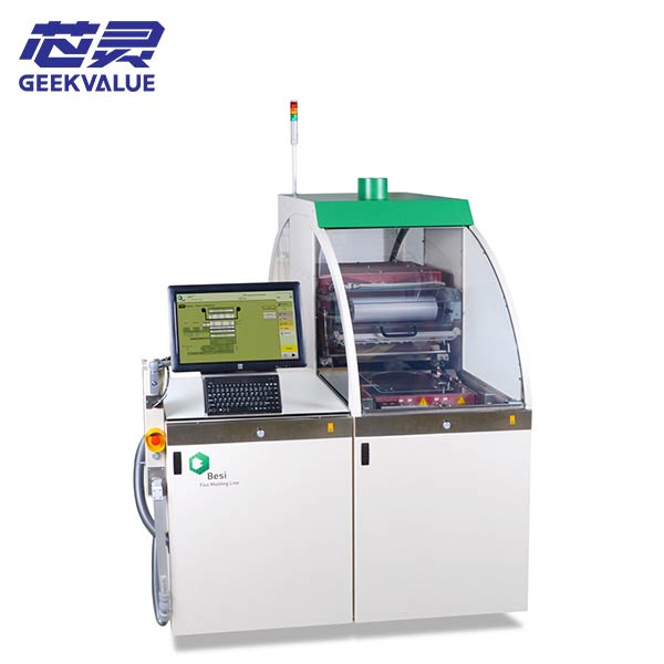
BESI ESEC 2100 hS is an automatic die bonder utilized in semiconductor backend packaging for epoxy die attach applications. It is engineered for stable mass production in OSAT and IDM manufacturing environments.
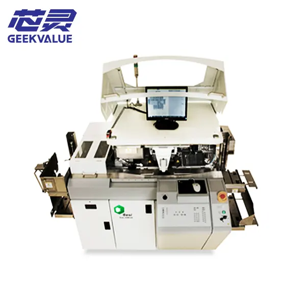
Key use cases: power semiconductors, automotive electronics, industrial ICs, and consumer semiconductor devices.
What is BESI ESEC 2100 hS?
The ESEC 2100 hS is a fully automatic die attach system used in semiconductor packaging to place silicon dies onto substrates or leadframes using epoxy bonding materials. It is designed to balance throughput and placement accuracy for mass production environments.
Key Specifications (Typical Industrial Configuration)
Specifications are highly dependent on process recipe, die size, and material handling configuration.
| Parameter | Typical Value |
|---|---|
| Throughput | Up to 18,500 UPH (process and material dependent) |
| Placement Accuracy | 15–20 μm @ 3σ (varies by die size and tooling) |
| Die Size Range | 0.25 mm – 20 mm |
| Wafer Support | Up to 12 inch (configuration dependent) |
| Bonding Type | Epoxy die attach |
Applications in Semiconductor Packaging Industry
The ESEC 2100 hS is deployed across mature semiconductor packaging production lines.
Power Semiconductor Packaging
MOSFET devices
IGBT modules
Power management ICs
Automotive Semiconductor Applications
Automotive MCUs
Sensor ICs
Power control modules
Consumer & Industrial Electronics
Memory chips
RF components
Industrial control ICs
Die Bonder vs Flip Chip Bonder
Different semiconductor packaging processes require distinct bonding technologies. The choice depends on interconnect density and packaging type.
| Feature | Die Bonder (ESEC 2100 hS) | Flip Chip Bonder |
|---|---|---|
| Process Type | Epoxy die attach (face-up) | Face-down flip chip bonding |
| Application Focus | Mainstream semiconductor packaging | Advanced packaging / High-performance computing |
| Throughput Priority | Optimized for high-volume production | Optimized for sub-micron precision alignment |
Why Semiconductor Manufacturers Use ESEC 2100 hS
Provides stable capability for high-volume production lines.
Represents a mature platform with established process parameters.
Suitable for long-lifecycle manufacturing with minimal process deviation.
Compatible with standard backend packaging flows and tooling.
Semiconductor Packaging Process Flow
Die attach using the ESEC 2100 hS is integrated into a complete backend semiconductor packaging sequence:
Wafer dicing
Die attach (ESEC 2100 hS)
Wire bonding
Molding
Singulation
Final test
Frequently Asked Questions (FAQ)
What is the main use of ESEC 2100 hS?
It is utilized for epoxy die attach processes within semiconductor backend packaging lines.
Is it still in active use today?
Yes, it remains in active use within mature production environments due to its process reliability and stable performance for standard package types.
What industries use this machine?
It is applied in automotive electronics, power semiconductors, industrial IC manufacturing, and consumer electronics packaging.
Can it be used for advanced packaging?
The platform is primarily designed for mainstream epoxy die attach. Advanced packaging typically requires dedicated flip chip bonding systems with higher precision capabilities.
Request Technical Specification or Quotation
If you are evaluating die attach equipment for semiconductor packaging production, our technical team can provide detailed machine specifications, configuration options, and process support.
👉 Contact us for:
Equipment specification sheet
Pricing & availability
Refurbished machine options
Process integration support
Email / Inquiry Form CTA Button