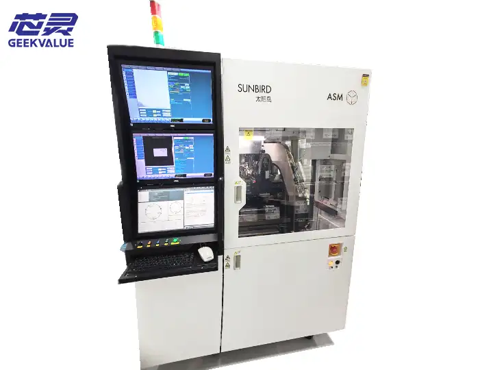
The ASMPT ALSI LASER1205 laser dicing machine is an advanced semiconductor wafer separation system designed for high-precision laser dicing and wafer grooving applications.
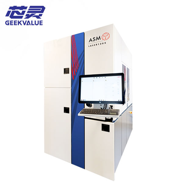
Developed by ASMPT ALSI, the LASER1205 platform uses multi-beam laser technology to achieve high-speed wafer processing with excellent edge quality, low thermal impact, and improved die strength.
Unlike traditional blade dicing systems, laser-based wafer separation reduces mechanical stress and enables semiconductor manufacturers to process challenging materials such as SiC, GaAs, Ge, thin silicon wafers, and advanced packaging materials.
The LASER1205 platform is designed for industrial semiconductor production environments, supporting automated wafer handling, inline inspection, and multiple laser configurations for different manufacturing requirements.
What is ASMPT ALSI LASER1205 Laser Dicing Machine?
The ASMPT ALSI LASER1205 is a fully automatic semiconductor laser processing system used for wafer dicing and grooving applications.
The equipment uses focused laser energy instead of mechanical cutting blades. This allows manufacturers to separate semiconductor wafers while minimizing mechanical stress and reducing edge damage.
The main applications include:
Semiconductor wafer dicing
Laser grooving
SiC wafer separation
GaAs wafer cutting
Thin wafer processing
Advanced semiconductor packaging
ASMPT ALSI developed the LASER1205 family as a high-volume manufacturing platform for wafer separation and grooving processes. The system is available in multiple configurations including Dicing UV Plus, Dicing IR, Grooving UV, and Grooving UV-USP. :contentReference[oaicite:0]{index=0}
Why Semiconductor Manufacturers Use Laser Dicing Technology
Traditional semiconductor wafer dicing mainly relies on diamond blade cutting. While blade dicing remains widely used, advanced semiconductor materials create new challenges because of their hardness, brittleness, and sensitivity to mechanical stress.
Laser dicing provides several advantages:
Lower mechanical stress
Reduced chipping and cracking
Narrower cutting width
Better die strength
Suitable for fragile semiconductor materials
This makes laser processing increasingly important for next-generation semiconductor applications including electric vehicle power devices, RF components, MEMS, and advanced packaging.
ASMPT ALSI LASER1205 Multi-Beam Laser Technology
Multi-Beam Laser Processing
The key technology of LASER1205 is ASMPT ALSI's multi-beam laser processing technology.
The system uses a Diffractive Optical Element (DOE) to divide the laser beam into multiple smaller beams. This allows multiple areas of the wafer to be processed simultaneously.
The multi-beam structure improves productivity while maintaining excellent cutting quality.
Low Heat Affected Zone (HAZ)
Heat generation is a critical issue during laser semiconductor processing.
Excessive thermal impact can affect semiconductor performance and reduce die reliability.
LASER1205 is designed to minimize the Heat Affected Zone (HAZ), supporting high-quality wafer separation for sensitive semiconductor devices.
ASMPT specifies typical LASER1205 performance values including positioning accuracy below 1.5 μm, cutting width below 12 μm, and low HAZ performance depending on process configuration. :contentReference[oaicite:1]{index=1}
ASMPT LASER1205 Machine Configurations
LASER1205 Dicing UV Plus
The UV Plus configuration is designed for thin silicon wafer dicing and high die-strength applications.
Typical applications include:
Power semiconductor devices
MOSFET
IGBT
Thin wafer processing
Advanced IC manufacturing
LASER1205 Dicing IR
The IR laser configuration is optimized for non-silicon semiconductor materials.
It is commonly used for:
GaAs wafer dicing
Ge wafer processing
RF semiconductor devices
The IR system uses a 1064 nm laser wavelength and supports high-quality processing of compound semiconductor materials. :contentReference[oaicite:2]{index=2}
LASER1205 Grooving UV
The Grooving UV configuration is designed to create precise grooves before blade dicing or plasma dicing processes.
It is commonly used for:
Low-K materials
Polyimide layers
Memory wafer preparation
LASER1205 Grooving UV-USP
The UV-USP configuration uses ultrashort pulse laser technology for advanced grooving applications.
It is designed for applications requiring extremely low thermal impact and precise material removal.
ASMPT LASER1205 Key Features
High Precision Wafer Processing
The LASER1205 is designed for semiconductor manufacturing environments where positioning accuracy and process stability are critical.
The system provides high-precision motion control to maintain stable laser processing quality during wafer separation and grooving operations.
High positioning accuracy helps manufacturers achieve consistent kerf quality and improve overall wafer yield.
Inline Vision Monitoring System
LASER1205 integrates an advanced vision inspection system for wafer alignment and process monitoring.
The vision system helps verify wafer position, monitor processing conditions, and improve production repeatability.
Real-time inspection reduces the risk of processing deviation during high-volume semiconductor production.
Automatic Wafer Handling
The equipment supports automated wafer loading, alignment, laser processing, and unloading.
The automated workflow reduces operator intervention and improves production efficiency.
Flexible Laser Source Options
Different semiconductor materials require different laser characteristics.
The LASER1205 platform supports multiple laser configurations including:
UV laser processing
IR laser processing
Ultrashort pulse laser processing
This flexibility allows manufacturers to optimize processes according to wafer material and device structure.
ASMPT LASER1205 Technical Specifications
| Parameter | Description |
|---|---|
| Equipment Type | Fully automatic semiconductor laser dicing and grooving system |
| Manufacturer | ASMPT ALSI |
| Model | LASER1205 |
| Processing Technology | Multi-beam laser dicing / laser grooving |
| Laser Configuration | UV / IR / UV-USP |
| Position Accuracy | Below 1.5 μm |
| Typical Kerf Width | Below 12 μm |
| Heat Affected Zone | Low thermal impact laser processing |
| Supported Materials | Silicon, SiC, GaAs, Ge, DAF, Mold materials |
| Main Applications | Wafer dicing, wafer grooving, semiconductor singulation |
The exact configuration depends on laser type, material requirements, and customer production process.
Applications of ASMPT LASER1205 Laser Dicing Machine
SiC Power Semiconductor Processing
Silicon carbide (SiC) has become a key material for next-generation power semiconductor devices used in electric vehicles, charging systems, and renewable energy applications.
Due to its high hardness and brittleness, SiC requires advanced wafer separation technology.
LASER1205 provides a low-damage laser processing solution for SiC wafer dicing and grooving.
GaAs RF Semiconductor Manufacturing
GaAs materials are widely used in RF communication devices, wireless systems, and high-frequency semiconductor applications.
Laser dicing helps reduce mechanical stress and improve die quality during GaAs wafer separation.
Advanced Packaging Applications
Modern semiconductor packaging requires thinner wafers and smaller die dimensions.
LASER1205 supports advanced packaging processes by providing narrow cutting widths and precise wafer processing capability.
Thin Wafer Processing
Thin silicon wafers are increasingly used in advanced semiconductor devices.
Mechanical cutting can introduce stress and cracks, while laser processing provides a lower-force alternative.
MEMS and Sensor Devices
MEMS devices often contain fragile structures that require low contamination and low mechanical stress processing.
Laser dicing technology provides advantages for these sensitive applications.
ASMPT LASER1205 vs DISCO DFL7341
| Comparison | ASMPT LASER1205 | DISCO DFL7341 |
|---|---|---|
| Technology | Multi-Beam Laser Dicing / Grooving | Stealth Dicing Technology |
| Main Advantage | High productivity and flexible laser processing | Low damage wafer separation |
| Main Materials | Si, SiC, GaAs, Ge, advanced packaging materials | Sapphire, SiC, MEMS, compound materials |
| Processing Method | Laser ablation / laser grooving | Internal laser modification layer |
| Typical Applications | Power semiconductor, RF, advanced packaging | LED, MEMS, compound semiconductor |
Both ASMPT LASER1205 and DISCO DFL7341 belong to advanced semiconductor laser processing equipment. However, their technical approaches are different.
LASER1205 focuses on flexible laser dicing and grooving productivity, while DFL7341 focuses on Stealth Dicing technology for low-damage wafer separation.
ASMPT LASER1205 Maintenance Considerations
Although laser dicing systems reduce mechanical wear compared with blade dicing equipment, regular maintenance is still required to maintain process stability.
Laser source performance inspection
Optical lens cleaning and alignment verification
Vision system calibration
Chuck table accuracy inspection
Motion axis calibration
Cooling system maintenance
Software and recipe backup
For refurbished ASMPT LASER1205 equipment, buyers should evaluate:
Laser source operating hours
Optical system condition
Processing accuracy records
Previous production applications
Maintenance history
Refurbished ASMPT LASER1205 Equipment Evaluation Guide
The semiconductor equipment second-hand market has increasing demand for laser dicing systems due to their high investment cost.
Before purchasing a refurbished LASER1205 system, engineers should confirm the following points:
| Inspection Item | Important Check |
|---|---|
| Laser System | Laser output stability and lifetime |
| Optical System | Lens condition and alignment accuracy |
| Motion System | X/Y/Z axis accuracy |
| Vision System | Camera calibration and recognition performance |
| Process Data | Previous wafer material and production history |
| Software | Recipe availability and system compatibility |
Conclusion
The ASMPT ALSI LASER1205 laser dicing machine is an advanced semiconductor wafer processing platform designed for modern semiconductor manufacturing requirements.
With multi-beam laser technology, flexible UV and IR configurations, automatic wafer handling, and support for difficult materials such as SiC and GaAs, LASER1205 provides a reliable solution for wafer dicing and laser grooving applications.
As semiconductor devices continue moving toward higher power density, smaller package sizes, and advanced materials, laser-based wafer processing technology will play an increasingly important role in semiconductor manufacturing.
Related Semiconductor Equipment
DISCO DFL7341 Laser Dicing System
DISCO DFD6341 Fully Automatic Dicing Saw
DISCO DFD6361 300mm Wafer Dicing Machine
DISCO DFG8830 SiC Wafer Grinder