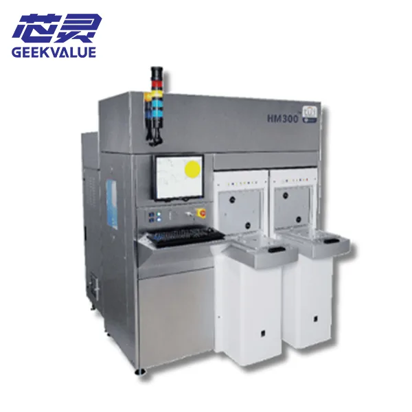
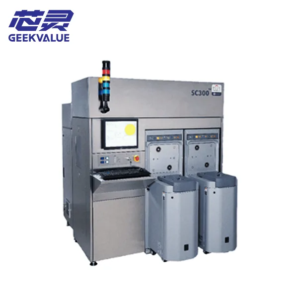
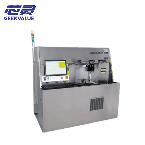
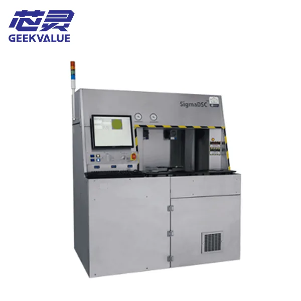
The ThinkLaser SigmaDSC is an automated laser marking system designed for permanent identification and traceability marking on semiconductor wafers.
Unlike general-purpose laser engraving machines, the SigmaDSC integrates precision laser marking, optical wafer alignment, automated wafer handling and production data control into a semiconductor-oriented platform.
The system creates durable dot-matrix hard marks directly on the wafer surface. These marks can help manufacturers maintain wafer identification throughout production, inspection, handling and logistics processes.
The ThinkLaser SigmaDSC is suitable for semiconductor fabs, silicon wafer manufacturers, foundries, wafer reclaim facilities, research laboratories and other production environments requiring reliable wafer-level identification.
Permanent Semiconductor Wafer Identification
Semiconductor wafers pass through numerous processing, inspection and material-handling stages. Reliable identification allows each wafer to be associated with its manufacturing lot, process history, inspection data and production records.
The SigmaDSC applies permanent laser marks directly to the wafer surface without using labels, ink or other temporary identification methods.
Typical marking content may include:
Wafer identification numbers
Lot numbers
Batch information
Serial numbers
Production tracking codes
Dot-matrix characters
Wafer ID codes
Customer-specific identification formats
Machine-readable marking structures
Permanent wafer identification helps manufacturers improve traceability and reduce the risk of wafers being mixed, incorrectly processed or associated with the wrong production data.
Semiconductor Wafer Hard Marking
The ThinkLaser SigmaDSC is primarily designed for permanent dot-matrix hard marking.
Hard marking creates controlled laser dots on the wafer surface. These dots form characters, numbers and other identification patterns that can remain readable during semiconductor manufacturing and wafer-handling processes.
The system supports different mark layouts, including:
Straight-line marking
Arc-shaped marking
Multiple marking groups
Different marking orientations
Wafer-edge identification
Custom character arrangements
Marking positions and formats can be programmed according to the production recipe and wafer identification requirements.
Programmable Marking Depth
The SigmaDSC provides programmable control over laser marking depth.
Marking depth can be adjusted according to the wafer material, marking format, process requirements and required level of permanence.
Representative configurations may support marking depths from approximately 5 μm to 110 μm. The actual available range depends on the installed laser source, optical system, software and equipment configuration.
Programmable depth control helps support:
Consistent mark formation
Permanent wafer identification
Repeatable marking results
Controlled laser penetration
Different wafer-product requirements
Stable results across production batches
The final marking parameters should be tested and qualified using the intended wafer material and downstream production process.
Configurable Laser Spot Size
The SigmaDSC can be configured with different laser spot sizes for different wafer marking requirements.
Depending on the installed optical configuration, representative spot diameters may range from approximately 50 μm to 110 μm.
Different spot sizes can be used to support variations in:
Character dimensions
Dot-matrix density
Marking depth
Wafer surface condition
Marking readability
Customer identification standards
Production requirements
Some configurations may provide software-selectable spot sizes, allowing operators to change marking parameters without replacing the complete optical system.
Consistent Dot Shape and Mark Quality
Reliable wafer identification depends on the quality and consistency of each laser-generated dot.
The SigmaDSC combines a stable laser source, precision optics and controlled process parameters to help maintain consistent dot depth, diameter and shape.
Consistent dot formation can improve:
Character readability
Machine-vision recognition
Marking repeatability
Process stability
Wafer traceability
Production quality control
Recognition of wafer identification codes
Marking quality depends on wafer material, surface condition, laser parameters, spot size, marking depth and equipment condition.
Automated Wafer Handling
The ThinkLaser SigmaDSC combines laser marking with automated wafer loading, alignment, positioning and unloading.
A typical equipment configuration may include:
High-resolution optical wafer aligner
Automated wafer-handling robot
Pick-and-place transfer mechanism
Single or dual robot end-effector
Multiple cassette-loading ports
Automatic wafer loading and unloading
Optional wafer-flipping hardware
Programmable job-file management
Integrated equipment control interface
Automated handling helps reduce direct operator contact with wafers and supports more consistent wafer positioning during production.
The actual wafer-handling configuration may vary according to the system manufacturing year, installed options and original production application.
Multiple Wafer-Size Support
The SigmaDSC platform can be configured for different semiconductor wafer sizes.
Depending on the installed cassette ports, robot hardware, aligner and handling components, representative configurations may support wafers from 100 mm to 300 mm.
Possible wafer sizes include:
100 mm wafers
125 mm wafers
150 mm wafers
200 mm wafers
300 mm wafers
Not every system supports all wafer sizes. Buyers should verify the actual installed handling hardware before purchasing a used or refurbished machine.
Important items to confirm include:
Cassette type
Cassette-port size
Robot end-effector
Wafer-aligner capability
Wafer thickness range
Wafer edge profile
Wafer-flipping capability
Software recipe support
Optical Wafer Alignment
Accurate marking placement requires precise wafer positioning and orientation.
The SigmaDSC uses an optical wafer-alignment system to identify wafer orientation and establish the correct marking reference before laser processing.
The alignment process helps control:
Marking position
Marking orientation
Distance from the wafer edge
Repeatability between wafers
Placement of multiple mark groups
Alignment with wafer flats or notches
Representative configurations may provide a marking field of approximately 50 × 50 mm after wafer alignment.
Actual positioning performance depends on the aligner condition, wafer type, software configuration and maintenance status.
High-Throughput Wafer Marking
The SigmaDSC is designed for automated production rather than manual single-wafer marking.
The integrated wafer robot, aligner and laser-marking system allow wafers to move through a coordinated processing sequence with limited operator handling.
Representative production configurations may achieve throughput of up to approximately 240 wafers per hour under specific marking conditions.
Actual throughput depends on:
Number of characters
Dot-matrix format
Marking depth
Wafer size
Number of marking groups
Wafer alignment time
Robot configuration
Loading and unloading sequence
Production recipe
Equipment condition
The final production output should be evaluated using the actual marking pattern and wafer-handling requirements.
Production Data and Recipe Management
The SigmaDSC uses programmable job files to manage wafer marking processes.
Operators can create and store different recipes for various wafer products, marking layouts and customer requirements.
Depending on the installed software version, the equipment may support:
Marking recipe storage
Job-file management
Character-format selection
Marking-depth settings
Spot-size selection
Wafer-size selection
Mark-position settings
Production quantity tracking
Equipment-status monitoring
Fault and alarm records
Process-data logging
Recipe management helps improve consistency when the same wafer product is processed repeatedly.
Closed-Loop Laser Monitoring
The SigmaDSC may include closed-loop laser monitoring and automatic performance-data logging.
These functions help production teams monitor laser operation and identify changes in marking performance.
System data may be used to support:
Laser performance monitoring
Process stability analysis
Preventive maintenance
Fault diagnosis
Production record management
Mark-quality investigation
Statistical process control
The available monitoring functions depend on the installed controller, software version and laser configuration.
Factory Automation Integration
The ThinkLaser SigmaDSC can be configured for integration with semiconductor factory automation systems.
Available communication functions may include SECS II/GEM connectivity, allowing compatible factory host systems to exchange information with the wafer laser marking machine.
Possible factory-integration functions include:
Equipment-status monitoring
Production job transfer
Recipe selection
Processing command control
Alarm reporting
Production-data collection
Wafer tracking
Host communication
Factory-level equipment management
The communication interface and software license should be verified before purchasing a used system.
Laser and Optical Configuration
Representative SigmaDSC systems may use a diode-pumped, Q-switched Nd:YLF laser source with a wavelength of approximately 1053 nm.
A typical laser and optical configuration may include:
Diode-pumped laser source
Q-switched pulse control
Nd:YLF laser technology
Flat-field focusing optics
Configurable laser spot size
Programmable marking depth
Closed-loop performance monitoring
Precision beam-delivery components
The exact laser model, optical hardware and operating condition may vary between machines.
Before purchase, buyers should verify:
Laser model
Laser manufacturing year
Laser operating hours
Laser output condition
Beam quality
Optical-lens condition
Marking-depth capability
Spot-size configuration
Cooling-system condition
Controller compatibility
Supported Wafer Materials
The ThinkLaser SigmaDSC is primarily intended for silicon wafer marking.
Representative applications may include:
Polished silicon wafers
Unpolished silicon wafers
Prime silicon wafers
Test wafers
Monitor wafers
Reclaimed wafers
Process-development wafers
Marking results may vary depending on:
Wafer material
Surface finish
Wafer coating
Laser wavelength
Laser power
Pulse settings
Marking depth
Spot diameter
Downstream processing conditions
Application testing is recommended before using the machine for specialty substrates, compound-semiconductor wafers or non-standard wafer materials.
Typical Applications
The ThinkLaser SigmaDSC can be used in semiconductor production processes requiring permanent wafer-level identification.
Silicon Wafer Manufacturing
Silicon wafer manufacturers can apply identification codes before wafers enter downstream semiconductor fabrication processes.
Permanent identification helps connect each wafer with its manufacturing lot, material specifications, inspection results and production records.
Semiconductor Fab Traceability
Semiconductor fabs can use wafer identification to associate each physical wafer with:
Process recipes
Production history
Inspection data
Equipment records
Manufacturing lot information
Quality-control results
Wafer Lot Identification
The machine can apply permanent lot, batch and serial information to wafers for improved production tracking.
Wafer Reclaim Operations
Wafer reclaim facilities can use permanent marking to identify incoming wafers, processing stages and completed wafer batches.
Research and Development
Semiconductor research centers and process-development laboratories can use automated marking to identify samples, experiments and qualification wafers.
Pilot Production
The system can support pilot production lines that require repeatable wafer identification and automated handling.
High-Volume Wafer Processing
Automated cassette loading and robotic wafer transfer make the system suitable for repeated production marking tasks.
Main Equipment Features
Automated semiconductor wafer laser marking
Permanent wafer hard marking
Dot-matrix character marking
Straight-line marking
Arc-shaped marking
Programmable marking depth
Configurable laser spot size
Optical wafer alignment
Automatic wafer loading
Automatic wafer unloading
Robotic wafer transfer
Multiple cassette-port configurations
Wafer ID marking
Production recipe storage
Job-file management
Process-data logging
Equipment alarm records
Factory automation connectivity
Semiconductor production traceability
Support for multiple wafer sizes
Suitable for polished and unpolished silicon wafers
Representative Technical Specifications
The following specifications are representative only. The actual machine configuration should be verified before purchase.
Marking method: Dot-matrix laser hard marking
Marking layout: Straight line or arc
Wafer size: Approximately 100 mm to 300 mm, configuration dependent
Wafer material: Polished and unpolished silicon
Dot diameter: Approximately 50 μm to 110 μm
Marking depth: Approximately 5 μm to 110 μm
Maximum characters: Configuration dependent
Marking field: Approximately 50 × 50 mm
Wafer alignment: Optical wafer aligner
Wafer transport: Automated pick-and-place robot
Laser type: Diode-pumped, Q-switched Nd:YLF
Laser wavelength: Approximately 1053 nm
Factory communication: SECS II/GEM, configuration dependent
Production throughput: Up to approximately 240 wafers per hour under specific conditions
Equipment application: Semiconductor wafer identification and traceability
Actual performance depends on the laser, optics, software, wafer-handling system and production recipe.
Equipment Configuration to Confirm
ThinkLaser SigmaDSC systems may have different configurations depending on manufacturing year, wafer size and original production application.
Before purchasing, buyers should confirm:
Equipment manufacturing year
Machine serial number
Current operational condition
Supported wafer sizes
Supported wafer thickness
Cassette-port configuration
Cassette compatibility
Robot type
Robot end-effector
Wafer-aligner condition
Wafer-flipping option
Laser model
Laser operating hours
Laser output condition
Optical-system condition
Available spot sizes
Marking-depth capability
Marking-format capability
Computer configuration
Operating-system version
Control-software version
Recipe availability
SECS II/GEM availability
Factory communication hardware
Maintenance history
Included manuals
Included accessories
Included spare parts
Power requirements
Cooling requirements
Exhaust requirements
Compressed-air requirements
Deinstallation status
Packaging and shipping scope
The model name alone does not confirm the complete wafer-size, laser, handling or software configuration of an individual machine.
Equipment Inspection and Supply Services
Available services may include:
Used semiconductor equipment sourcing
Equipment-condition inspection
Wafer-size configuration verification
Laser-source inspection
Optical-system inspection
Wafer-handler evaluation
Robot-function testing
Wafer-aligner inspection
Software-version verification
Communication-interface verification
Deinstallation coordination
Export packing
International transportation
Installation coordination
Spare-parts sourcing
Technical consultation
The final service scope depends on the equipment condition, location and project requirements.
Why Choose the ThinkLaser SigmaDSC?
The ThinkLaser SigmaDSC is designed specifically for semiconductor wafer marking rather than general-purpose industrial engraving.
Its combination of permanent hard marking, automated wafer handling, optical alignment, programmable marking depth and production-data management makes it suitable for facilities requiring controlled wafer identification.
The system can help manufacturers reduce manual wafer handling while maintaining repeatable marking positions, character formats and production recipes.
It is particularly suitable for semiconductor manufacturing environments where wafer traceability, equipment automation and marking consistency are important.
Frequently Asked Questions
What is the ThinkLaser SigmaDSC used for?
The ThinkLaser SigmaDSC is used to apply permanent identification marks to semiconductor wafers for production tracking, lot management and wafer-level traceability.
Is the SigmaDSC a hard-marking machine?
Yes. The SigmaDSC is primarily designed for permanent dot-matrix hard marking on semiconductor wafers.
Which wafer sizes can the SigmaDSC process?
Depending on the installed handling configuration, the machine may support wafer sizes from approximately 100 mm to 300 mm.
Can the machine process 300 mm wafers?
Some SigmaDSC configurations may support 300 mm wafers. The cassette ports, robot, aligner and software configuration must be verified.
Can the marking depth be adjusted?
Yes. The marking depth can be programmed according to the wafer material and production requirements.
What type of laser does the system use?
Representative systems may use a diode-pumped, Q-switched Nd:YLF laser with a wavelength of approximately 1053 nm.
Can it mark polished silicon wafers?
Representative configurations may support both polished and unpolished silicon wafers. Application testing is recommended for the intended wafer type.
Does the system support automated wafer handling?
Yes. The machine can integrate wafer cassette loading, robotic transfer, optical alignment, laser marking and automatic unloading.
Can the system connect to factory automation?
Some configurations may support SECS II/GEM communication for connection to compatible semiconductor factory host systems.
What should be checked before purchasing a used SigmaDSC?
Buyers should verify the wafer-size configuration, laser condition, robot operation, cassette ports, wafer aligner, optical system, software version, factory interface, maintenance history and included accessories.
Request ThinkLaser SigmaDSC Equipment Information
Looking for a ThinkLaser SigmaDSC semiconductor wafer laser marking system?
Send us your required wafer size, marking format, production application, preferred equipment condition and destination country.
We can provide available equipment information, machine photos, configuration details, condition information and a quotation based on your project requirements.