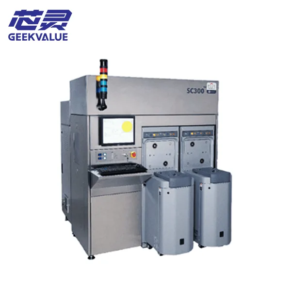
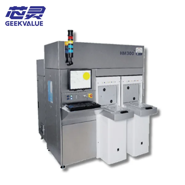
The ThinkLaser HM300 is an automated semiconductor wafer laser marking system designed for permanent hard marking on 300 mm silicon wafers.
Built for production environments where wafer identification must remain readable after demanding semiconductor processes, the HM300 creates precise dot-matrix marks directly on the wafer surface. It combines laser marking, optical alignment, automated wafer handling, programmable mark-depth control and production data management in one integrated platform.
Unlike soft-marking systems that focus primarily on shallow, low-debris marks, the HM300 is designed to produce deeper and more durable identification marks. This makes it suitable for semiconductor manufacturing processes involving repeated cleaning, thermal treatment, chemical exposure, inspection or wafer reclaim operations.
The system can be used by semiconductor fabs, silicon wafer manufacturers, foundries, wafer reclaim facilities, research centers and other companies that require reliable wafer-level identification and traceability.
Permanent Hard Marking for Semiconductor Wafers
The HM300 uses controlled laser pulses to create permanent physical marks on the wafer surface.
Each character is formed from a series of precisely positioned laser dots. These dots can be arranged into numbers, letters, barcodes, two-dimensional codes and other wafer identification formats.
Typical marking content may include:
Wafer identification numbers
Production lot numbers
Batch numbers
Serial numbers
Manufacturing codes
Process tracking information
Equipment or production references
Dot-matrix characters
BC-412 barcodes
Two-dimensional data matrix codes
Customer-specific wafer IDs
Because the identification is marked directly onto the wafer, it does not depend on labels, ink or other removable marking methods.
Permanent wafer identification helps manufacturers connect each physical wafer with its production history, process recipes, inspection results and quality-control records.
Durable Marks for Demanding Wafer Processes
The main purpose of wafer hard marking is to create identification that remains readable after challenging downstream production processes.
Potential downstream processes may include:
Wafer cleaning
Chemical treatment
Thermal processing
Surface processing
Wafer polishing
Material removal
Metrology and inspection
Reclaim processing
Repeated production handling
Long-term material storage
The required marking depth depends on the wafer material, surface condition and subsequent production process.
A deeper mark may provide greater durability, while a shallower recipe may be selected when less wafer-surface modification is required. The final process should be tested using the intended wafer type and manufacturing flow.
Programmable Mark-Depth Control
The ThinkLaser HM300 provides programmable control over the depth of each laser-generated dot.
Representative configurations support dot depths from approximately 5 μm to 110 μm. This wide adjustment range allows users to create different marking recipes for different wafer products and process requirements.
Programmable depth control can help provide:
Adjustable mark permanence
Consistent dot depth
Controlled wafer-surface modification
Repeatable marking results
Support for different wafer products
Compatibility with different downstream processes
Reduced variation between production lots
Greater process flexibility
The correct depth should be selected according to the required mark durability and the acceptable level of wafer-surface modification.
Dual-Spot Optics Technology
The HM300 can be equipped with Dual-Spot Optics technology.
This design allows two calibrated laser spot sizes to be used on the same machine. The required spot size can be selected through the system software according to the active production recipe.
Depending on the installed laser and optical configuration, representative spot sizes range from approximately 50 μm to 110 μm.
Dual-spot capability provides additional flexibility for applications requiring different:
Dot diameters
Character sizes
Dot-matrix densities
Marking depths
Identification formats
Wafer products
Customer specifications
Production processes
The actual spot sizes available on an individual machine should be confirmed before purchase.
Controlled Dot Diameter and Shape
Each wafer ID character consists of multiple laser-generated dots. The diameter, depth and shape of these dots directly affect mark readability and production consistency.
Representative HM300 marking capabilities include:
Dot diameters from approximately 50 μm to 110 μm
Dot depths from approximately 5 μm to 110 μm
Controlled dot roundness
Programmable process parameters
Stable laser pulse output
Repeatable dot-matrix formation
Consistent dot formation helps improve:
Character clarity
Machine-vision recognition
Marking repeatability
Wafer identification accuracy
Lot-to-lot consistency
Process stability
Statistical process control
Actual dot quality depends on the wafer material, laser condition, optical alignment, equipment calibration and selected marking recipe.
Top-Side and Bottom-Side Marking
The ThinkLaser HM300 can support top-side or bottom-side wafer marking requirements, depending on the installed wafer-handling configuration.
This gives manufacturers greater flexibility when identification must be placed according to a specific wafer design, production standard or downstream process.
The marking side may be selected based on:
Active device areas
Wafer edge-exclusion requirements
Downstream processing
Inspection requirements
Existing wafer identification
Customer marking standards
Factory traceability rules
The exact top-side or bottom-side handling capability of an available machine should be verified from its installed hardware and software configuration.
Dedicated 300 mm Wafer Processing
The HM300 is primarily designed for automated processing of 300 mm semiconductor wafers.
A representative equipment configuration may include:
Two 300 mm cassette ports
Automated wafer loading
Pick-and-place wafer robot
Single robot end effector
High-resolution optical wafer aligner
Controlled laser-marking enclosure
Automatic wafer unloading
Integrated production software
The automated handling system moves wafers between the cassette ports, alignment station and laser-marking position with limited operator contact.
This helps improve wafer-positioning consistency while reducing the risk associated with manual wafer handling.
Optional 200 mm Bridge Capability
Selected HM300 machines may include optional hardware for processing 200 mm wafers.
A 200 mm conversion or bridge configuration may require:
Compatible cassette adapters
Wafer-size bridge hardware
Appropriate robot end effector
Optical-aligner support
Software recipe configuration
Wafer-handling qualification
Additional accessories
Not every HM300 machine can automatically process both 200 mm and 300 mm wafers.
The actual wafer-size capability should be confirmed from the installed cassette ports, robot hardware, aligner configuration and included accessories.
Polished and Unpolished Silicon Wafer Support
The ThinkLaser HM300 is designed for permanent marking on polished and unpolished silicon wafers.
Typical wafer applications may include:
Polished silicon wafers
Unpolished silicon wafers
Prime wafers
Monitor wafers
Test wafers
Process-development wafers
Reclaimed silicon wafers
Marking results may vary according to:
Wafer material
Surface finish
Surface coating
Laser absorption
Dot diameter
Laser pulse settings
Required marking depth
Downstream production processes
Application testing is recommended before processing specialty materials such as silicon carbide, gallium arsenide, sapphire, glass or coated semiconductor wafers.
Optical Wafer Alignment
Accurate mark placement requires the wafer position and orientation to be identified before laser processing.
The HM300 uses a high-resolution optical wafer aligner to locate the primary wafer reference and establish the correct marking position.
Optical alignment helps control:
Wafer notch position
Wafer orientation
Marking angle
Distance from the wafer edge
Straight-line mark placement
Arc-shaped mark placement
Multiple marking groups
Repeatability between wafers
Representative mark-position repeatability is approximately ±75 μm in the X and Y directions relative to the primary wafer reference.
Actual alignment performance depends on the wafer condition, aligner calibration, robot condition and maintenance status.
Straight-Line and Arc Marking
The ThinkLaser HM300 supports both straight-line and arc-shaped dot-matrix marking.
Straight-line marking is commonly used for conventional wafer ID strings, serial numbers, lot numbers and production codes.
Arc marking allows the identification content to follow the curved circumference of the wafer.
Available marking arrangements may include:
Straight wafer ID strings
Arc-shaped wafer-edge marks
Multiple marking groups
Different character orientations
Primary and secondary wafer IDs
Barcode placement
Data matrix placement
Customer-defined marking locations
The marking layout can be programmed according to the wafer design and production requirements.
Multiple Marking Groups
The HM300 can place multiple identification groups at different locations and orientations on the wafer.
Representative configurations allow marks to be positioned within an approximately 25 mm band around the wafer circumference.
This provides flexibility for applications requiring:
Internal and customer identification codes
Primary and secondary wafer IDs
Human-readable and machine-readable information
Separate lot and wafer numbers
Different mark orientations
Multiple production references
Barcode and character combinations
The system can support up to approximately 80 characters per marking group, depending on the selected font and layout.
SEMI-Compatible Marking Formats
The ThinkLaser HM300 is designed to support marking formats used in semiconductor wafer manufacturing.
Representative formats include:
5 × 9 SEMI single-density dot matrix
9 × 17 single-density dot matrix
10 × 18 double-density dot matrix
T1 BC-412 barcode
T7 two-dimensional data matrix
M12 character formation
M13 character formation
User-selectable checksum
Custom marking fonts
The available formats depend on the control software installed on the machine.
When evaluating used equipment, buyers should verify the software version, marking libraries, custom fonts and factory-interface licenses.
Marking Field and Position Control
Representative HM300 configurations provide a marking field of approximately 50 × 50 mm after wafer alignment.
Marking can be positioned within an approximately 25 mm band around the wafer circumference.
Controlled marking placement helps support:
Standardized wafer IDs
Controlled edge positioning
Reduced interference with active wafer areas
Multiple identification groups
Arc-shaped character placement
Barcode positioning
Data matrix positioning
Repeatability across production lots
The final marking position should be selected according to wafer design, edge-exclusion zones and downstream process requirements.
Automated Wafer Handling
The HM300 integrates wafer transport, alignment and laser marking into a coordinated automated process.
A typical operating sequence may include:
Selecting a wafer from the cassette
Automatically picking up the wafer
Transferring it to the optical aligner
Detecting the wafer notch and orientation
Moving the wafer to the laser-marking position
Applying the selected marking recipe
Returning the marked wafer to the assigned cassette
Automated wafer handling helps provide:
Reduced manual wafer contact
Consistent wafer positioning
Repeatable marking orientation
Controlled production flow
Improved lot tracking
Higher processing efficiency
Reduced handling-related contamination risk
The robot, end effector, cassette ports and optical aligner should be inspected when evaluating used equipment.
Production Throughput
The HM300 is designed for automated semiconductor production.
Representative throughput is approximately 65 to 85 wafers per hour under a defined marking condition using a single-pulse, 5 × 9 dot-matrix and 12-character identification mark.
Actual production throughput depends on:
Number of characters
Dot-matrix format
Marking depth
Selected spot size
Number of marking groups
Straight or arc marking
Wafer-alignment time
Robot movement
Cassette configuration
Host-system communication
Equipment condition
Production capacity should be evaluated using the customer’s actual wafer type, marking content and qualified recipe.
Closed-Loop Laser Control
The ThinkLaser HM300 combines its laser source with system-level closed-loop control.
This helps the equipment monitor laser performance and maintain more consistent marking results during production.
Closed-loop control can support:
Laser pulse monitoring
Marking-energy stability
Dot-depth control
Dot-diameter consistency
Recipe repeatability
Laser-performance tracking
Process variation analysis
Preventive maintenance planning
Representative laser pulse stability is below approximately 0.5% at 1 kHz.
The performance of an available machine should be confirmed through inspection and wafer-marking tests.
Automated Data Logging
The HM300 can automatically record laser and system-performance information.
This information can support statistical process control, production traceability and equipment maintenance.
Available data-management functions may include:
Laser-performance records
Marking job history
Production quantity records
Process recipe storage
Equipment alarm logs
Fault and error records
System diagnostic information
Mark-quality data
Equipment-status monitoring
Data logging helps production teams investigate process changes and identify potential marking-performance issues.
Production Recipe Management
The HM300 uses programmable job files to manage different wafer products and marking requirements.
A production recipe may include:
Wafer size
Marking content
Character format
Dot-matrix density
Barcode or data matrix selection
Marking position
Marking orientation
Laser spot size
Marking depth
Number of marking groups
Cassette assignment
Production quantity
Host communication settings
Multiple job-file storage helps operators repeat qualified marking processes across different wafer lots.
SECS II/GEM Factory Integration
The ThinkLaser HM300 can include a SECS II/GEM communication interface for connection with semiconductor factory host systems.
Possible factory-integration functions include:
Equipment-status monitoring
Production job transfer
Remote recipe selection
Processing commands
Alarm reporting
Event reporting
Production-data collection
Wafer tracking
Host-controlled operation
Factory-level equipment management
The communication hardware, control-software version and license status should be verified before purchasing an available machine.
Laser and Optical System
Representative HM300 systems use an acousto-optic Q-switched, diode-pumped Nd:YLF laser.
Typical laser and optical characteristics include:
Diode-pumped laser source
Acousto-optic Q-switching
TEM00 beam mode
Approximately 1053 nm wavelength
Flat-field focusing lens
Configurable laser spot size
Programmable marking depth
Closed-loop laser monitoring
Stable pulse output
Before purchasing used equipment, buyers should verify:
Laser model
Laser serial number
Laser manufacturing year
Laser operating hours
Laser-output condition
Pulse stability
Beam quality
Optical-lens condition
Beam alignment
Available spot sizes
Marking-depth capability
Cooling-system condition
Controller compatibility
Wafer-marking test results
Cleanroom-Compatible Construction
The ThinkLaser HM300 is designed for installation in semiconductor cleanroom environments.
Representative construction includes a stainless steel enclosure compatible with an ISO Class 5 cleanroom and an ISO Class 2 mini-environment around the controlled wafer-processing area.
Cleanroom-oriented features may include:
Stainless steel equipment enclosure
Enclosed laser-processing area
Controlled wafer-handling environment
Mark-point exhaust connection
Process vacuum connection
Static-charge control
Automated wafer transfer
Reduced manual wafer contact
The actual cleanroom condition of a used system should be evaluated before installation.
Previous operating environment, deinstallation method, storage conditions and equipment maintenance may affect its suitability.
Main Equipment Features
Automated 300 mm wafer laser marking
Permanent semiconductor wafer hard marking
Programmable marking depth
Dot-matrix character marking
Straight-line marking
Arc-shaped marking
Dual-Spot Optics technology
User-selectable laser spot sizes
Top-side or bottom-side marking configurations
SEMI-compatible marking formats
Barcode marking
Two-dimensional data matrix marking
Multiple marking-group placement
Optical wafer alignment
Automatic wafer loading and unloading
Two 300 mm cassette ports
Pick-and-place wafer robot
Optional 200 mm bridge capability
Polished and unpolished silicon wafer support
Closed-loop laser control
Automated process-data logging
Multiple job-file storage
Fault and error logging
SECS II/GEM factory communication
Cleanroom-compatible construction
High-durability wafer identification
Representative Technical Specifications
The following specifications are representative. The actual configuration and performance of an available machine should be verified before purchase.
Marking method: Dot-matrix laser hard marking
Marking layout: Straight line or arc
Primary wafer size: 300 mm
Optional wafer capability: 200 mm bridge
Wafer materials: Polished and unpolished silicon
Dot diameter: Approximately 50–110 μm
Dot depth: Approximately 5–110 μm
Dot-depth tolerance: Approximately ±10%
Dot roundness: Less than approximately 1.1 major-to-minor axis ratio
Maximum characters: Up to 80 characters per marking group
Marking field: Approximately 50 × 50 mm after alignment
Marking position: Within a 25 mm band around the wafer circumference
Mark repeatability: Approximately ±75 μm in X and Y
Character formation: SEMI M12 and M13
Standard formats: T1 barcode and T7 two-dimensional data matrix
Wafer alignment: High-resolution optical wafer aligner
Wafer transport: Pick-and-place robot with single end effector
Cassette ports: Two 300 mm ports
Laser type: Acousto-optic Q-switched, diode-pumped Nd:YLF
Laser wavelength: Approximately 1053 nm
Pulse stability: Less than approximately 0.5% at 1 kHz
Optical system: Flat-field focusing lens
Representative throughput: Approximately 65–85 wafers per hour
Factory communication: SECS II/GEM
Certification configuration: CE and applicable SEMI requirements
Representative System Dimensions
Representative equipment dimensions are:
Height: Approximately 1981 mm
Width: Approximately 1641 mm
Depth: Approximately 1204 mm
EFEM weight: Approximately 671 kg
Marking enclosure weight: Approximately 519 kg
The complete shipping dimensions and packed weight may be higher after adding accessories, protective materials and export crates.
Dimensions should be confirmed before planning cleanroom access, transportation and installation.
Representative Utility Requirements
Facility requirements may vary according to the exact machine configuration.
Representative requirements include:
Electrical supply: 200–240 VAC
Phase: Single phase
Frequency: 50/60 Hz
Rated current: Approximately 23 FLA
Process vacuum: Required
Mark-point exhaust: Required
Maximum exhaust flow: Approximately 20 CFM
Exhaust-port diameter: Approximately 50.8 mm
Operating temperature: Approximately 12.8–27°C
Network connection: Required for host communication
Static-charge control: According to facility requirements
All utility requirements should be confirmed from the nameplate and documentation of the actual machine before installation.
Equipment Configuration to Confirm
ThinkLaser HM300 systems may have different configurations depending on manufacturing year, original customer requirements and previous production use.
Before purchasing, buyers should confirm:
Equipment manufacturing year
Machine serial number
Current operational condition
Supported wafer sizes
Optional 200 mm bridge hardware
Top-side or bottom-side marking configuration
Cassette-port condition
Cassette compatibility
Wafer-robot condition
Robot end-effector condition
Optical-aligner condition
Wafer-notch compatibility
Laser model and serial number
Laser operating hours
Laser-output condition
Optical-system condition
Available laser spot sizes
Marking-depth capability
Supported marking fonts
Barcode capability
Two-dimensional data matrix capability
Computer configuration
Operating-system version
Control-software version
Recipe availability
SECS II/GEM availability
Factory-interface license
Data-logging capability
Process-vacuum condition
Exhaust requirements
Maintenance history
Included documentation
Included accessories
Included spare parts
Current installation status
Deinstallation scope
Packing and transportation requirements
The HM300 model name alone does not confirm the complete configuration of an individual machine.
Typical Applications
Semiconductor Fab Wafer Traceability
Semiconductor fabs can use permanent wafer IDs to connect physical wafers with process recipes, inspection results, equipment records and manufacturing history.
Silicon Wafer Manufacturing
Silicon wafer manufacturers can apply durable identification before wafers are delivered to downstream semiconductor fabrication facilities.
Processes Requiring Durable Marks
Programmable hard marking is suitable for processes where identification must remain readable after cleaning, thermal treatment, surface processing or other demanding manufacturing steps.
High-Volume 300 mm Wafer Production
Automated cassette ports, robotic wafer transfer and optical alignment allow the HM300 to support repeated production marking with limited operator handling.
Wafer Lot and Batch Management
Lot numbers, serial numbers and production codes can be marked directly onto individual wafers to improve material control and traceability.
Wafer Reclaim Operations
Wafer reclaim facilities can use permanent identification for incoming inspection, processing control and outgoing batch management.
Research and Process Qualification
Semiconductor laboratories and process-development facilities can use the HM300 to identify engineering wafers, test samples and qualification lots.
Why Choose the ThinkLaser HM300?
The ThinkLaser HM300 is designed specifically for permanent hard marking of 300 mm semiconductor wafers.
Its programmable marking depth allows process engineers to select an appropriate balance between identification durability and controlled wafer-surface modification.
The combination of Dual-Spot Optics, automated wafer handling, optical alignment, closed-loop laser control and factory communication makes the system suitable for manufacturing environments that require consistent wafer identification.
Compared with a general-purpose laser marking machine, the HM300 provides wafer-specific handling, semiconductor marking formats, controlled mark placement and cleanroom-oriented construction.
It is particularly suitable for facilities where wafer identification must remain readable after demanding downstream semiconductor processes.
Frequently Asked Questions
What is the ThinkLaser HM300 used for?
The HM300 is used to create permanent dot-matrix hard marks on semiconductor wafers for production identification, lot management and wafer-level traceability.
Is the HM300 a hard-marking or soft-marking system?
The HM300 is a hard-marking system. It produces deeper and more durable marks than a semiconductor wafer soft-marking platform.
Which wafer size does the HM300 process?
The standard HM300 is designed for 300 mm wafers. Selected machines may include optional 200 mm bridge capability.
Can every HM300 process 200 mm wafers?
No. The machine must include compatible bridge hardware, cassette components, wafer-handling equipment and software support.
Which wafer materials can the HM300 mark?
Representative configurations support both polished and unpolished silicon wafers. Other substrates should be evaluated through application testing.
What is the representative marking-depth range?
Representative configurations provide programmable dot depths from approximately 5 μm to 110 μm.
Can the HM300 create arc-shaped marks?
Yes. The system supports both straight-line and arc-shaped dot-matrix marking.
Does the HM300 support more than one spot size?
Selected machines include Dual-Spot Optics technology, allowing two software-controlled spot sizes to be used on the same system.
Can the machine mark the top or bottom of a wafer?
The HM300 can support top-side or bottom-side marking configurations. The installed wafer-handling setup should be confirmed on the individual machine.
Does the HM300 support automated wafer handling?
Yes. A representative configuration includes two 300 mm cassette ports, an optical aligner and an automated pick-and-place wafer robot.
Does the HM300 support factory communication?
The system can include a SECS II/GEM interface for communication with compatible semiconductor factory host systems.
What should be checked before purchasing a used HM300?
Buyers should inspect the laser source, marking quality, wafer robot, cassette ports, optical aligner, available spot sizes, marking-depth capability, software version, factory interface and maintenance history.
Request ThinkLaser HM300 Equipment Information
Looking for a ThinkLaser HM300 semiconductor wafer laser marking system?
Send us your required wafer size, marking depth, character format, wafer material, production application, preferred equipment condition and destination country.
We can provide available machine photos, equipment configuration, condition information, technical details and a quotation based on your project requirements.