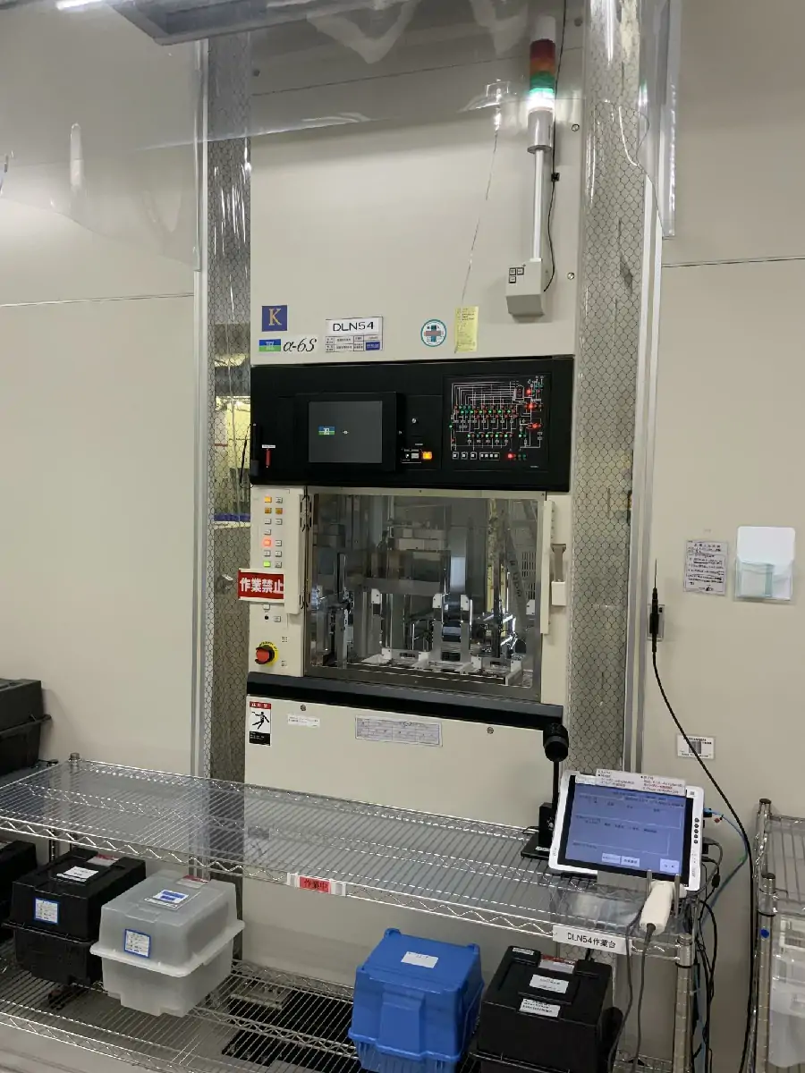
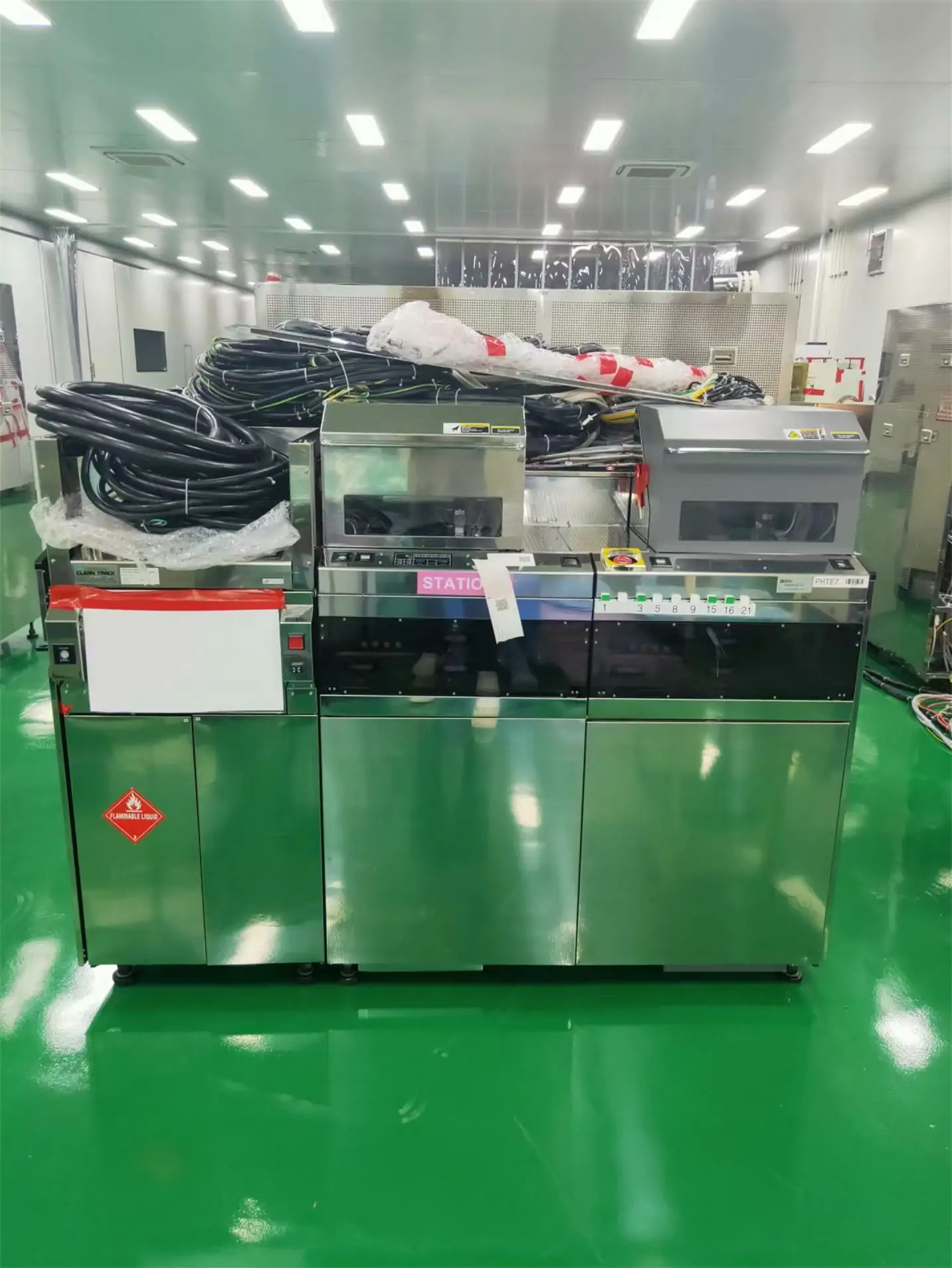
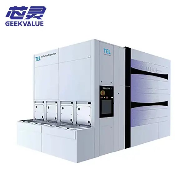
The Tokyo Electron TEL MARK 8 is a wafer coater and developer designed for photoresist processing in semiconductor photolithography. The available equipment listing identifies it for 6-inch and 8-inch wafer processing in a listed 2C+2D configuration.
The system is intended to coat wafers before exposure and develop the resist pattern after exposure. As used MARK 8 systems can differ in process modules, thermal units, chemical delivery and wafer interfaces, the installed configuration should be inspected before purchase.
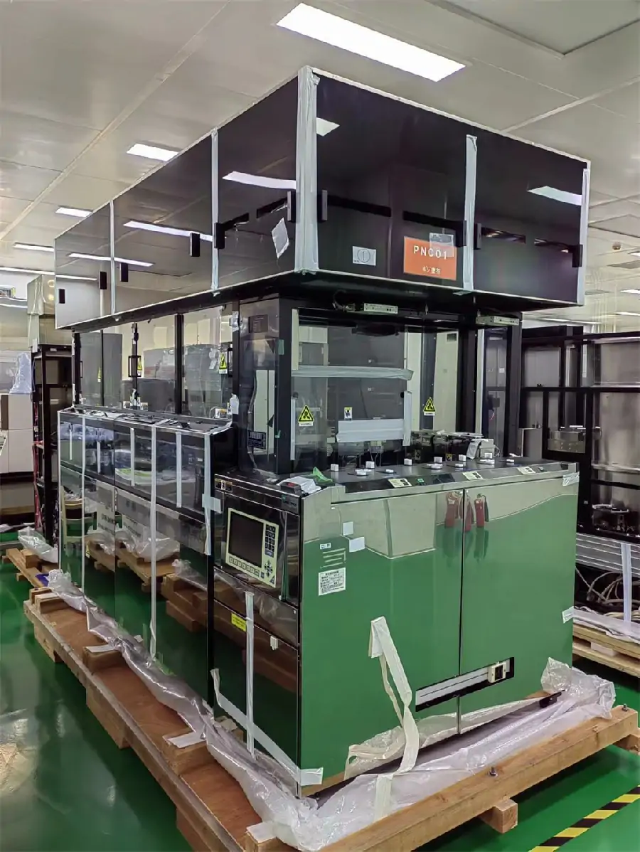
TEL MARK 8 Main Specifications
| Manufacturer | Tokyo Electron Limited |
|---|---|
| Brand | TEL |
| Model | MARK 8 |
| Equipment Type | Wafer Coater and Developer Track System |
| Supported Wafer Sizes | 6-inch and 8-inch wafers, according to the available listing |
| Listed Process Configuration | 2C+2D; actual installed modules must be confirmed |
| Primary Process | Photoresist coating and developing |
| Condition | Used semiconductor equipment |
| Availability | Subject to current stock and configuration confirmation |
Key Equipment Features
Supports listed 150 mm and 200 mm wafer processing
Combines photoresist coating and developing operations
Listed with a 2C+2D process configuration
Suitable for use in established photolithography production lines
Individual used-machine modules and delivery scope can vary
Typical Applications
The TEL MARK 8 may be used for wafer priming, photoresist coating, thermal treatment and development as part of a photolithography sequence. The exact supported process flow depends on the installed process and thermal modules.
Potential applications include integrated circuit fabrication, MEMS processing, discrete semiconductor manufacturing and other 150 mm or 200 mm wafer processes requiring automated resist coating and development.
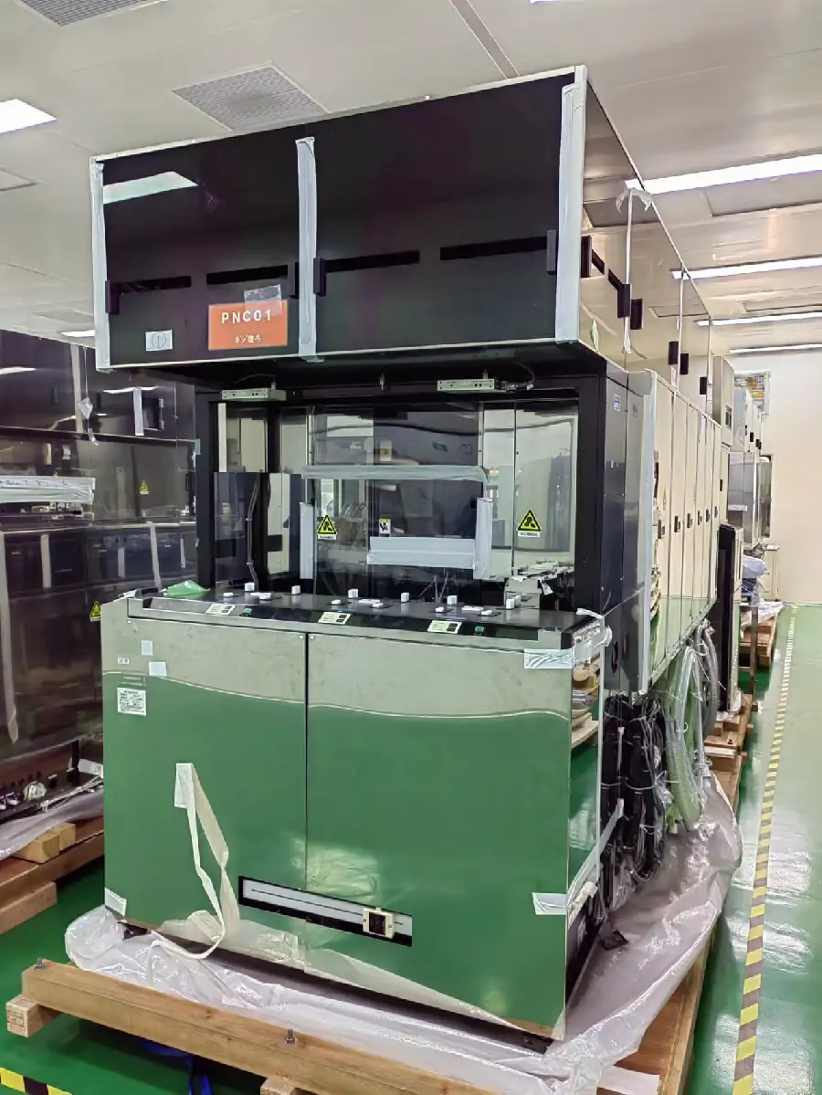
Used Equipment Configuration and Inspection
The source listing describes the system as 2C+2D, but this does not identify every hot plate, cool plate, cassette station, chemical line or automation option installed on the machine. These items should be confirmed from current equipment photos and the component list.
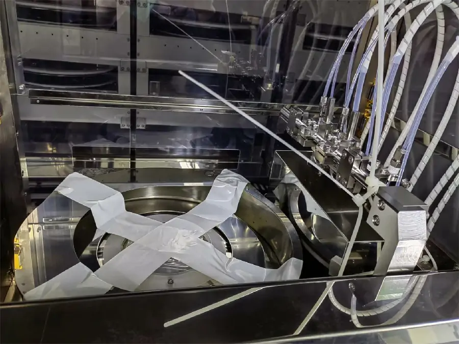
Before quotation, customers should verify the serial number, wafer-size setup, cassette stations, wafer robot, coating bowls, developing modules, thermal units, chemical cabinet, environmental controls, software condition and current power-on status.
Request TEL MARK 8 Information
Contact our team to check the current availability of the used TEL MARK 8. Please provide your wafer diameter, photoresist and developer requirements, required process modules, exposure tool, destination country and expected installation schedule.
Contact us for current photos, installed configuration, delivery scope, inspection status and quotation.
Frequently Asked Questions
What wafer sizes can the TEL MARK 8 process?
The available listing identifies the system for 6-inch and 8-inch wafers. The installed wafer-handling hardware should be checked for the required size.
What does the listed 2C+2D configuration indicate?
It indicates coating and developing process modules in the seller listing. The exact module count, layout and operating condition should be confirmed during inspection.
Can the MARK 8 be installed with an existing stepper?
Installation depends on wafer size, cassette standards, track-to-stepper interface, software communication and facility layout. Compatibility should be evaluated for the specific exposure tool.
What should be inspected before purchasing a used MARK 8?
Important checks include wafer transfer, spin motors, coating and developing cups, thermal plates, chemical delivery, temperature control, safety interlocks and system software.