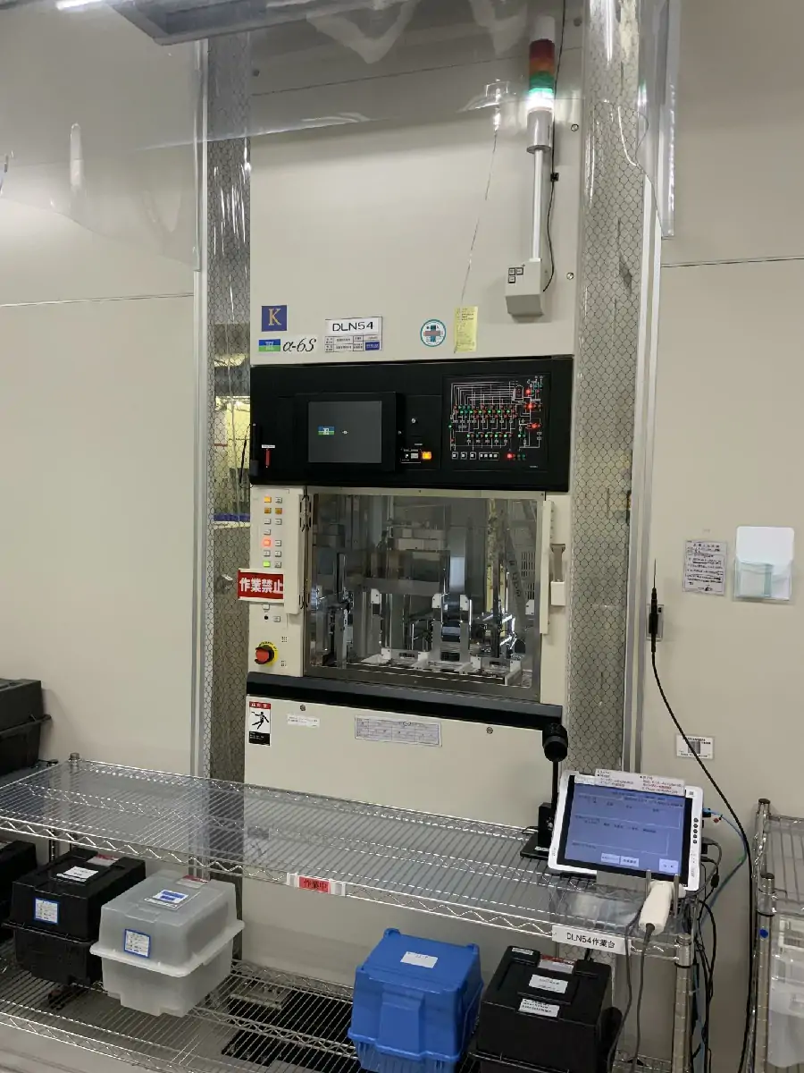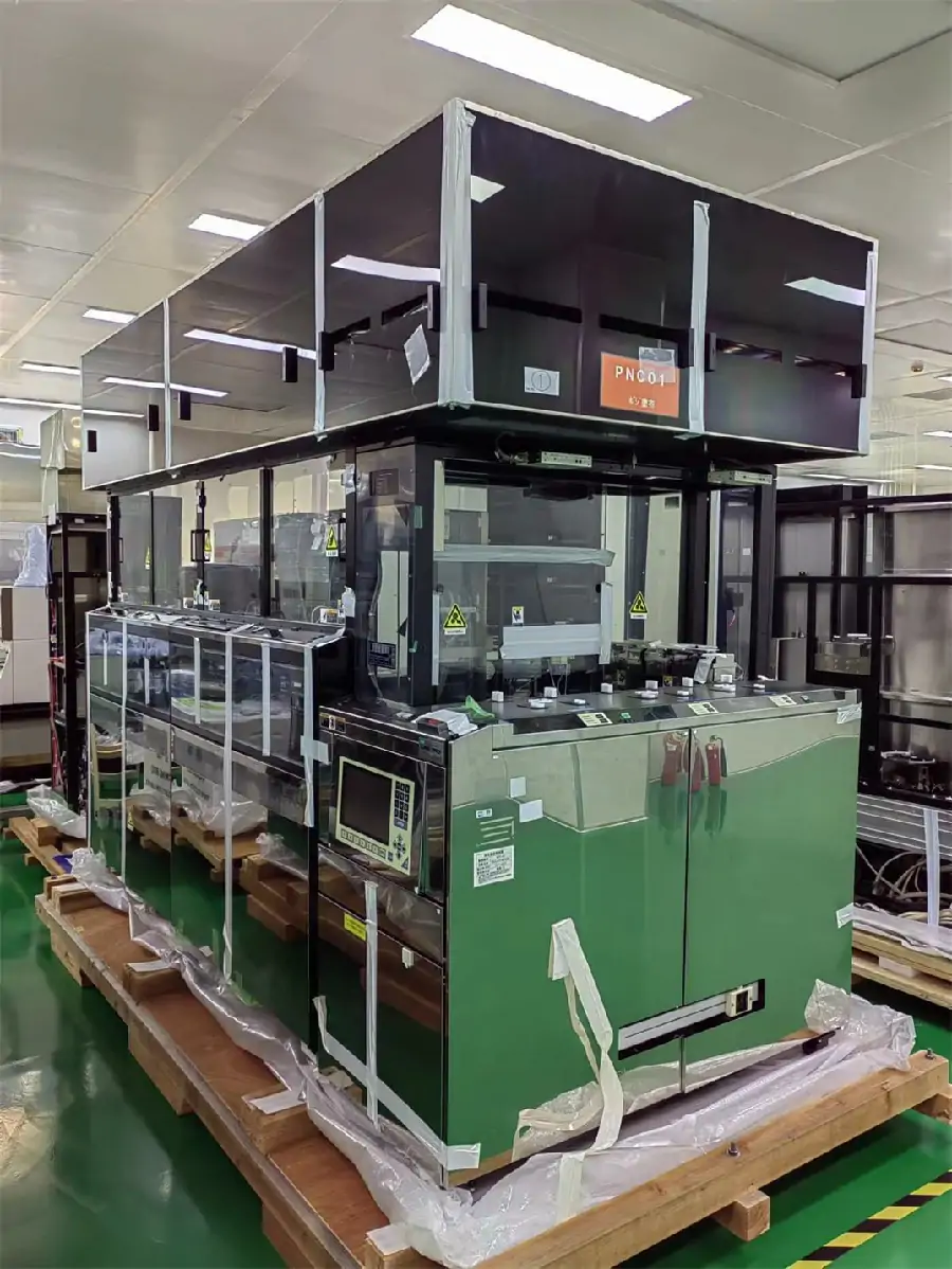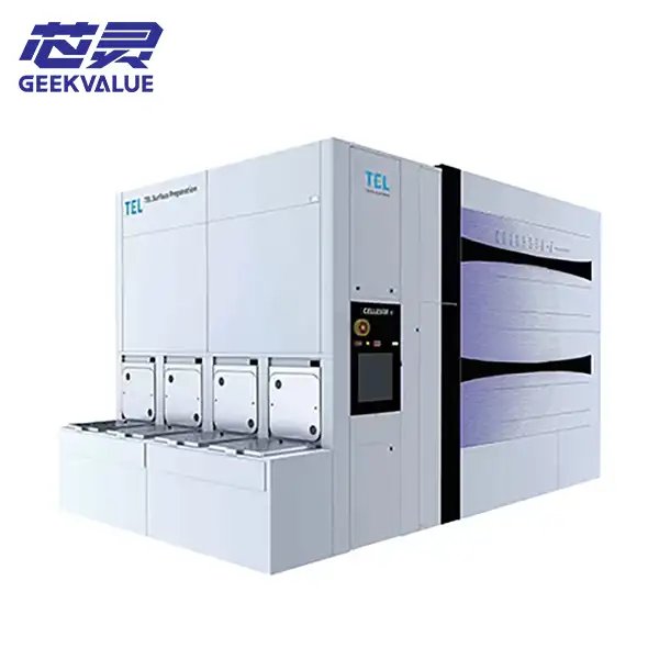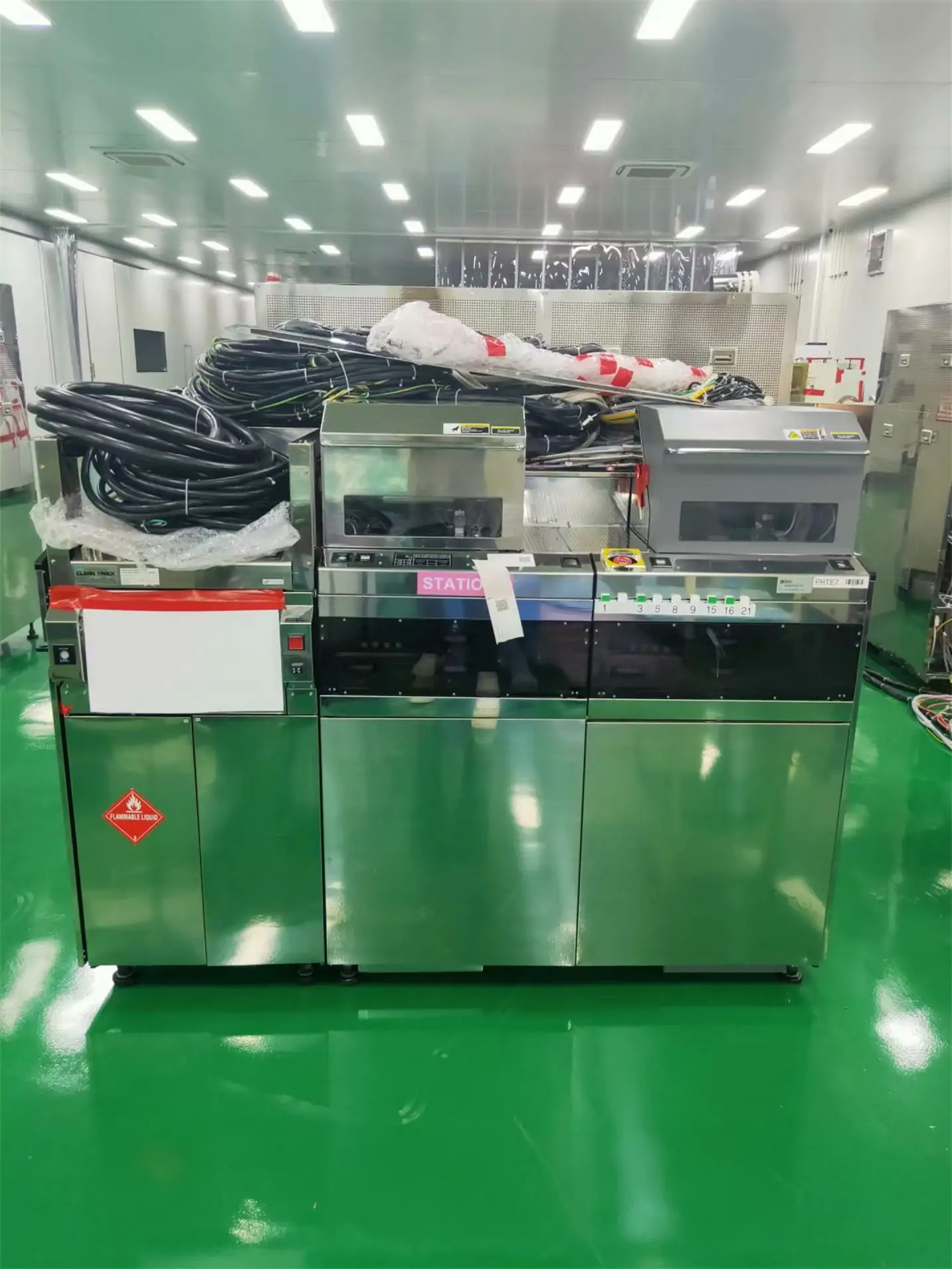
The Tokyo Electron TEL MARK Vz is a wafer coater and developer used for photoresist processing in semiconductor photolithography. The available listing identifies this system for 6-inch wafer processing with a listed 2C and 2D configuration.
The MARK Vz platform combines resist coating and developing functions with wafer handling and supporting chemical and environmental systems. The exact process-module arrangement, thermal configuration and interface condition should be verified on the available equipment.
TEL MARK Vz Main Specifications
| Manufacturer | Tokyo Electron Limited |
|---|---|
| Brand | TEL |
| Model | MARK Vz |
| Equipment Type | Wafer Coater and Developer Track System |
| Supported Wafer Size | 6-inch wafers, according to the available listing |
| Listed Process Configuration | 2C and 2D; actual installed modules must be confirmed |
| Primary Process | Photoresist coating and developing |
| Condition | Used semiconductor equipment |
| Availability | Subject to current stock and configuration confirmation |
Key Equipment Features
-
Designed for 150 mm wafer photolithography processing
-
Combines photoresist coating and developing functions
-
Source listing identifies 2C and 2D process capability
-
Separate chemical supply and environmental support sections may be included
-
Suitable for established semiconductor and research process lines
Typical Applications
The TEL MARK Vz can apply photoresist to 150 mm wafers, support the required coating process sequence and develop the resist after lithography exposure. The platform may be used in semiconductor device fabrication, MEMS processing and other compatible wafer-level photolithography applications.
Actual process support depends on the installed coating and developing modules, thermal plates, resist supply, developer delivery, wafer-handling configuration and software recipes.
Used Equipment Configuration and Inspection
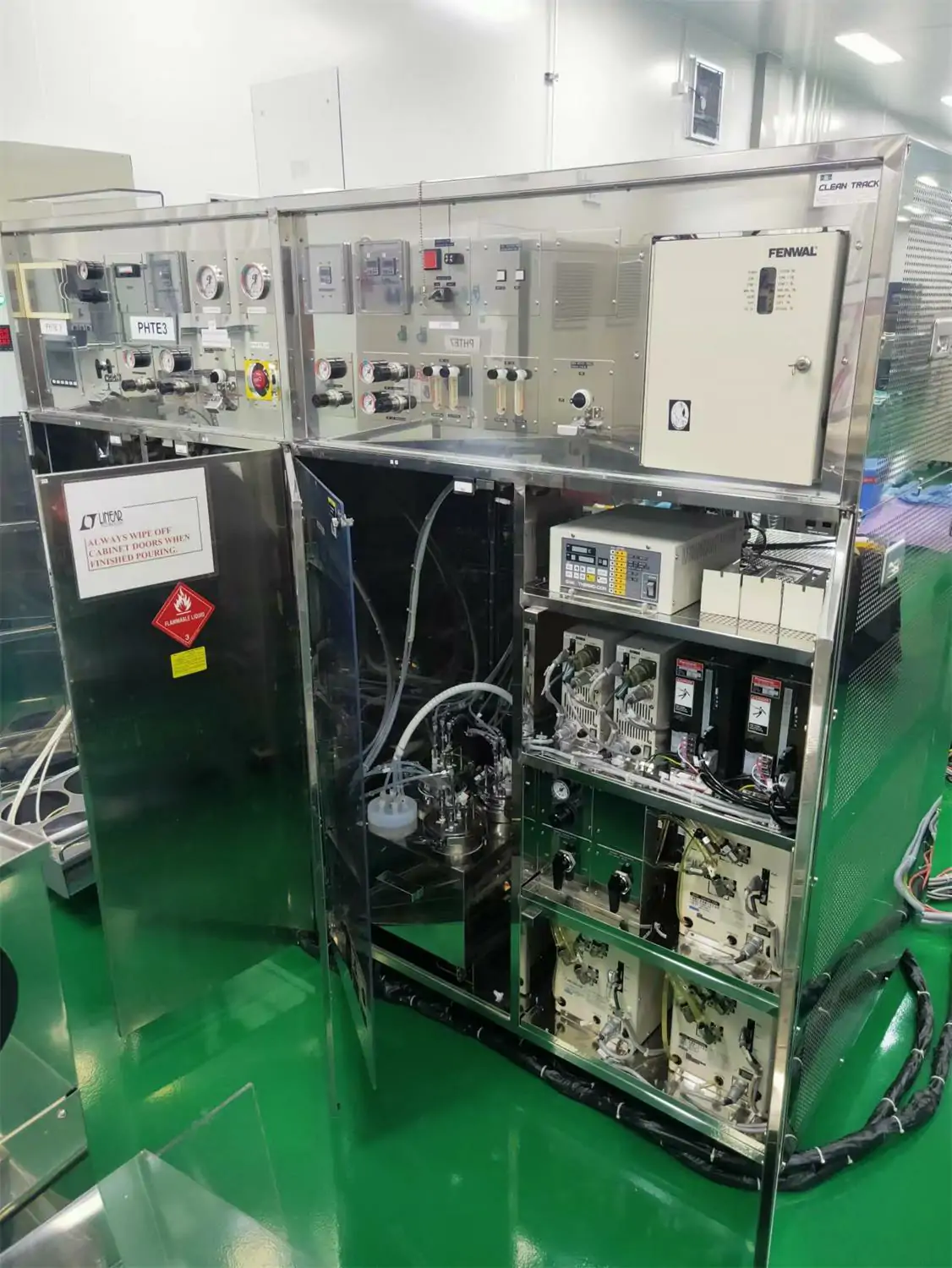
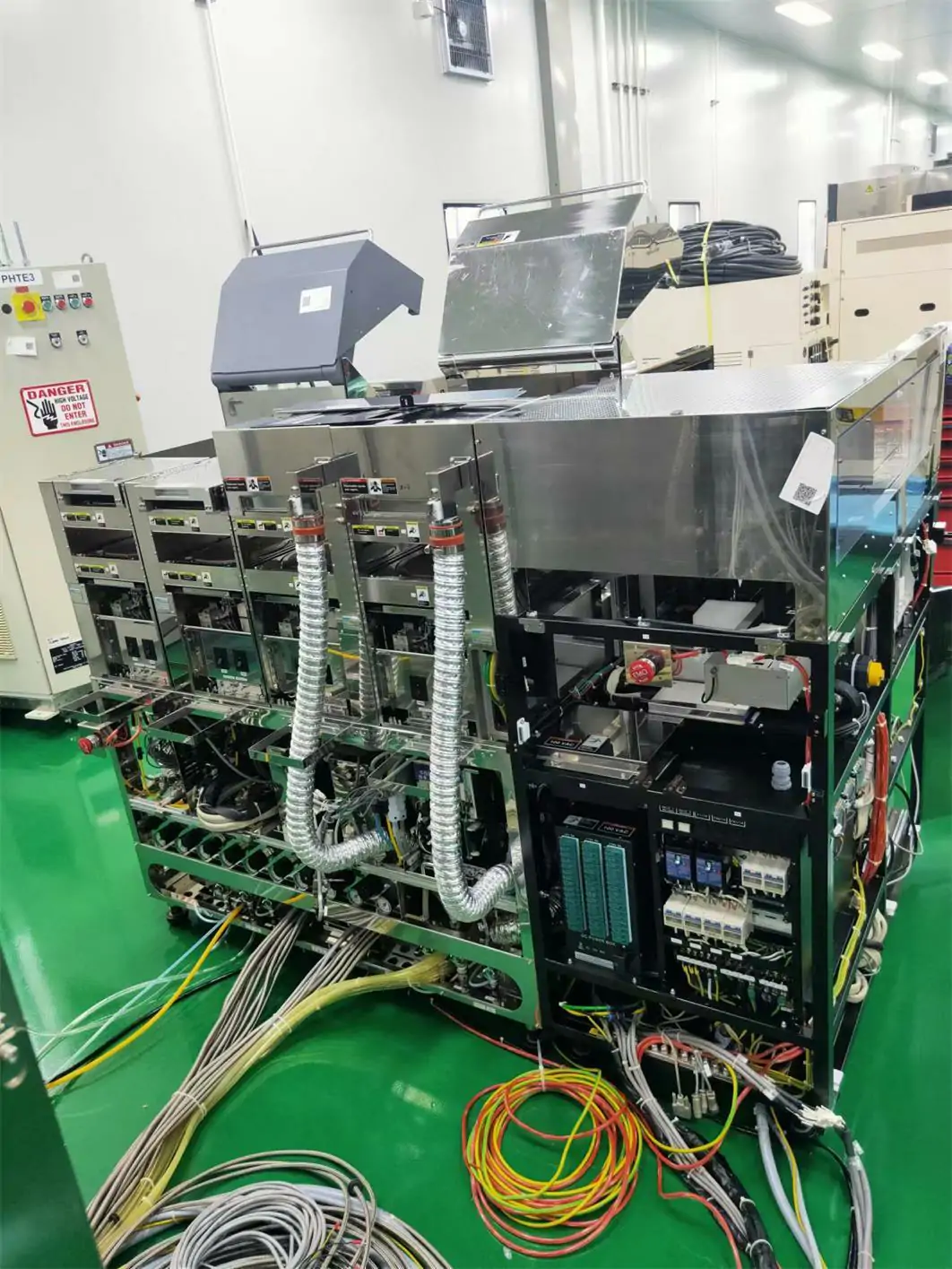
The available source images identify a main system, environmental or air-conditioning cabinet, rear connections and a chemical supply cabinet. All sections required for operation should be compared with the final delivery list.
Before quotation, customers should confirm the machine serial number, process modules, hot and cool plates, wafer robot, cassette stations, chemical cabinet, temperature-control equipment, exhaust connections, control software and current power-on status.
Request TEL MARK Vz Information
Contact our team to check the current availability of the used TEL MARK Vz. Please provide your wafer size, photoresist type, required coat-and-develop process, exposure tool interface, destination country and installation schedule.
Contact us for machine photos, installed modules, delivery scope, inspection status and quotation.
Frequently Asked Questions
What wafer size does the TEL MARK Vz process?
The available listing identifies this MARK Vz configuration for 6-inch wafers. The cassette and wafer-handling parts should be checked before final confirmation.
Is the MARK Vz a coating-only machine?
The listing identifies it as a coater and developer with 2C and 2D process capability. The exact module arrangement must be verified on the individual system.
Does the system include its chemical supply cabinet?
The source page shows a chemical supply cabinet, but the complete included scope should be confirmed in the quotation and equipment delivery list.
Can the TEL MARK Vz connect to an exposure tool?
Integration depends on the wafer interface, track configuration, software communication and the selected lithography system. Compatibility should be reviewed for the intended production line.